Stress enhanced mos transistor and methods for its fabrication

a technology of mos transistor and mos, which is applied in the field of stress enhanced mos transistor and its fabrication, can solve the problems of increasing the complexity of ics and the number of devices incorporated in ics, increasing the loss of sige from the surface, and increasing the performance of individual devices, so as to achieve enhanced majority carrier mobility and greater thickness

Active Publication Date: 2008-05-22
INNOVATIVE FOUNDRY TECH LLC
View PDF14 Cites 47 Cited by
  • Summary
  • Abstract
  • Description
  • Claims
  • Application Information

AI Technical Summary

Benefits of technology

[0006]A stress enhanced MOS transistor having enhanced majority carrier mobility is provided. The stress enhanced MOS transistor comprises a semiconductor substrate having a surface and a channel region at the surface. A first region of SiGe having a first germanium concentration is embedded in the semiconductor substrate. The first region has a bottom portion and a side portion adjacent the channel region. A second region of SiGe having a second germanium concentration less than the first germanium concentration is embedded in the first region so that the side portion has a greater thickness than the bottom portion.

Problems solved by technology

The complexity of ICs and the number of devices incorporated in ICs are continually increasing.
As the semiconductor industry moves to a minimum feature size of 45 nanometers (nm) and even smaller, the performance of individual devices degrades as the result of scaling.
Simply increasing the germanium content of the eSiGe to increase the stress, however, is not entirely successful as increased germanium content results in increased SiGe loss from the surface of the embedded region, agglomeration of the metal silicide formed on the embedded region to reduce contact resistance to the source and drain areas, and increased stress relaxation of the embedded material as the transistor undergoes the more conventional steps encountered in fabricating the IC.

Method used


Image

  • Stress enhanced mos transistor and methods for its fabrication
  • Stress enhanced mos transistor and methods for its fabrication
  • Stress enhanced mos transistor and methods for its fabrication

Examples


Embodiment Construction

[0011]The following detailed description is merely exemplary in nature and is not intended to limit the invention or the application and uses of the invention. Furthermore, there is no intention to be bound by any expressed or implied theory presented in the preceding technical field, background, brief summary or the following detailed description.

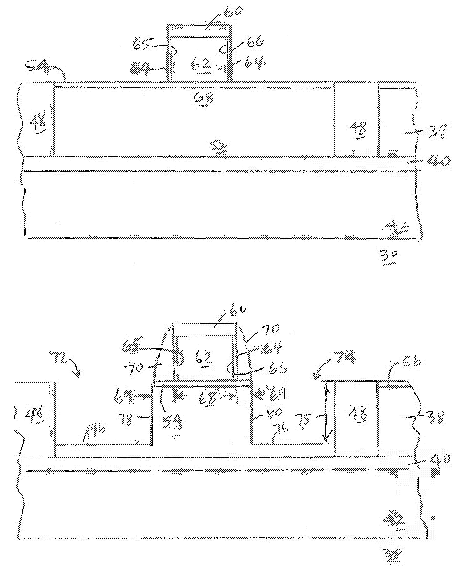
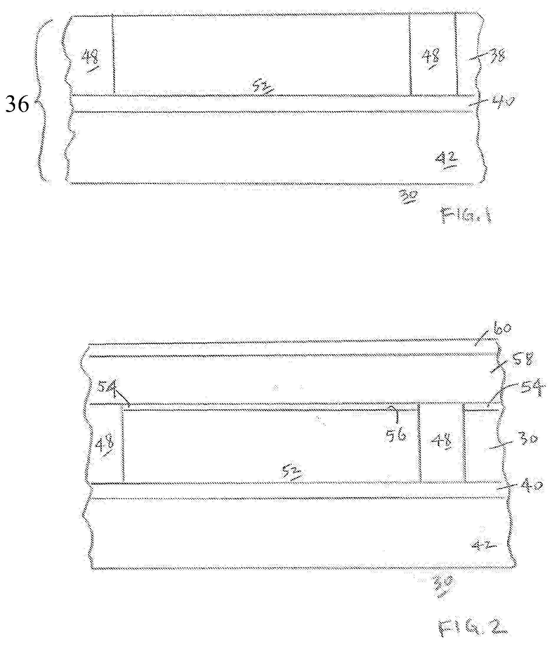
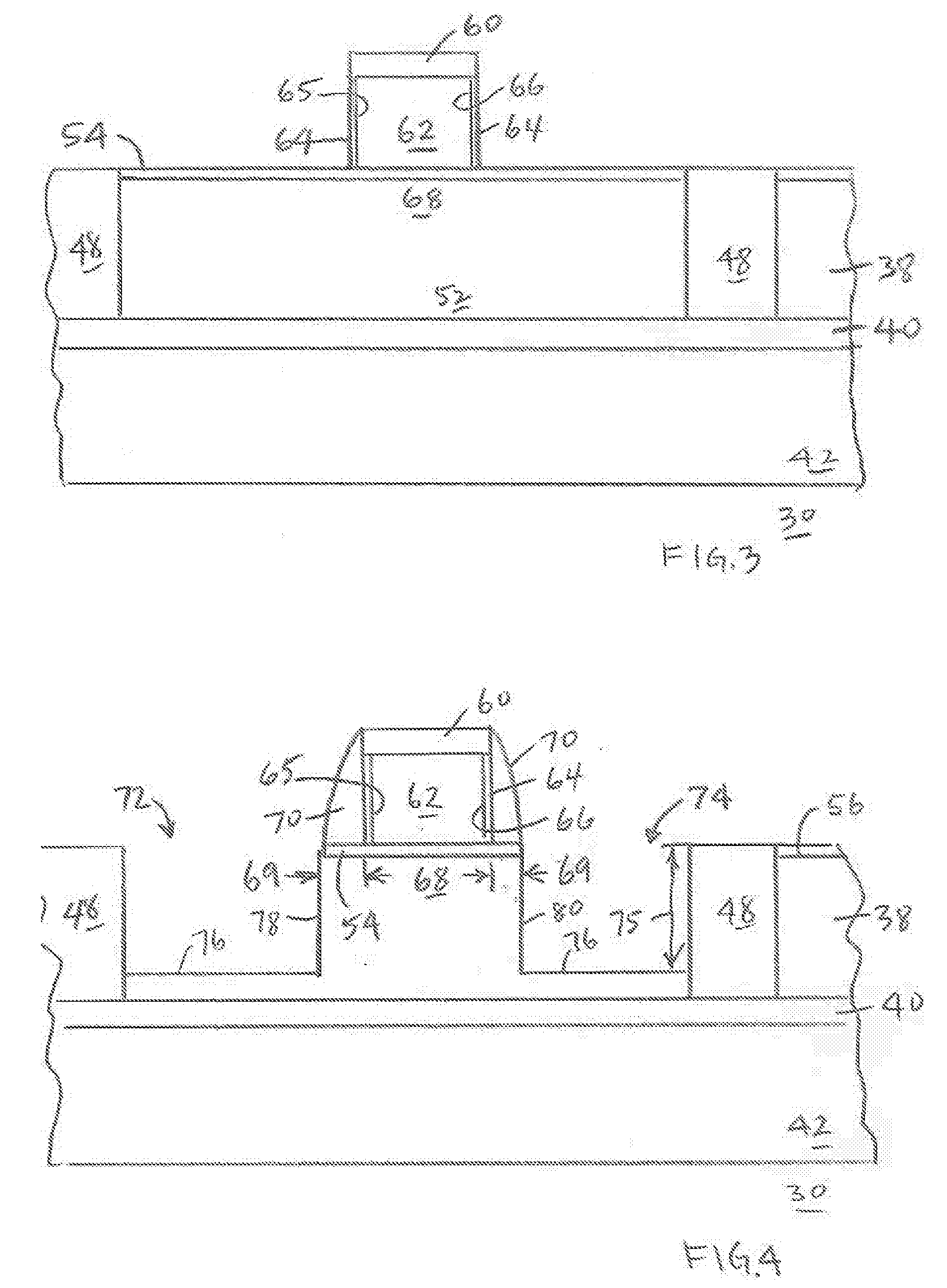
[0012]Monocrystalline silicon, the most common semiconductor material used in the semiconductor industry for the fabrication of semiconductor devices and integrated circuits is characterized by a lattice constant, a dimension of the silicon crystal. By substituting atoms other than silicon in a crystal lattice, the size of the resulting crystal and the lattice constant can be changed. If a larger substitutional atom such as a germanium atom is added to the silicon lattice, the lattice constant increases and the increase in lattice constant is proportional to the concentration of the substitutional atom. Similarly, if a smaller substitution...


PUM


Abstract

A stress enhanced MOS transistor and methods for its fabrication are provided. In one embodiment the method comprises forming a gate electrode overlying and defining a channel region in a monocrystalline semiconductor substrate. A trench having a side surface facing the channel region is etched into the monocrystalline semiconductor substrate adjacent the channel region. The trench is filled with a second monocrystalline semiconductor material having a first concentration of a substitutional atom and with a third monocrystalline semiconductor material having a second concentration of the substitutional atom. The second monocrystalline semiconductor material is epitaxially grown to have a wall thickness along the side surface sufficient to exert a greater stress on the channel region than the stress that would be exerted by a monocrystalline semiconductor material having the second concentration if the trench was filled by the third monocrystalline material alone.

Description

TECHNICAL FIELD[0001]The present invention generally relates to MOS transistors and to methods for their fabrication, and more particularly relates to stress enhanced MOS transistors and to methods for fabricating such transistors with embedded material adjacent the transistor channel.BACKGROUND[0002]The majority of present day integrated circuits (ICs) are implemented by using a plurality of interconnected field effect transistors (FETs), also called metal oxide semiconductor field effect transistors (MOSFETs), or simply MOS transistors. An MOS transistor includes a gate electrode as a control electrode and spaced apart source and drain electrodes between which a current can flow. A control voltage applied to the gate electrode controls the flow of current through a channel between the source and drain electrodes.[0003]The complexity of ICs and the number of devices incorporated in ICs are continually increasing. As the number of devices in an IC increases, the size of individual d...

Claims


Application Information

Patent Timeline
Patent Type & Authority Applications(United States)
IPC IPC(8): H01L21/20H01L21/36H01L31/20
CPCH01L21/02532H01L21/02639H01L21/823807H01L29/7848H01L29/045H01L29/165H01L29/66636H01L21/823814H01L21/18H01L29/04
Inventor PAL, ROHITPEIDOUS, IGORBROWN, DAVID
Owner INNOVATIVE FOUNDRY TECH LLC
Why Eureka
Try Eureka