
Heat processing apparatus for semiconductor process

a technology of heat processing apparatus and semiconductor, which is applied in the direction of coating, chemical vapor deposition coating, metallic material coating process, etc., can solve the problems of particle contamination, difficult to form films with high uniformity among the target substrates, and increase the gap between the reaction tube and the target substrate, so as to achieve the effect of improving the planar uniformity of the film thickness

Active Publication Date: 2008-04-10
TOKYO ELECTRON LTD
View PDF14 Cites 27 Cited by
  • Summary
  • Abstract
  • Description
  • Claims
  • Application Information

AI Technical Summary

Benefits of technology

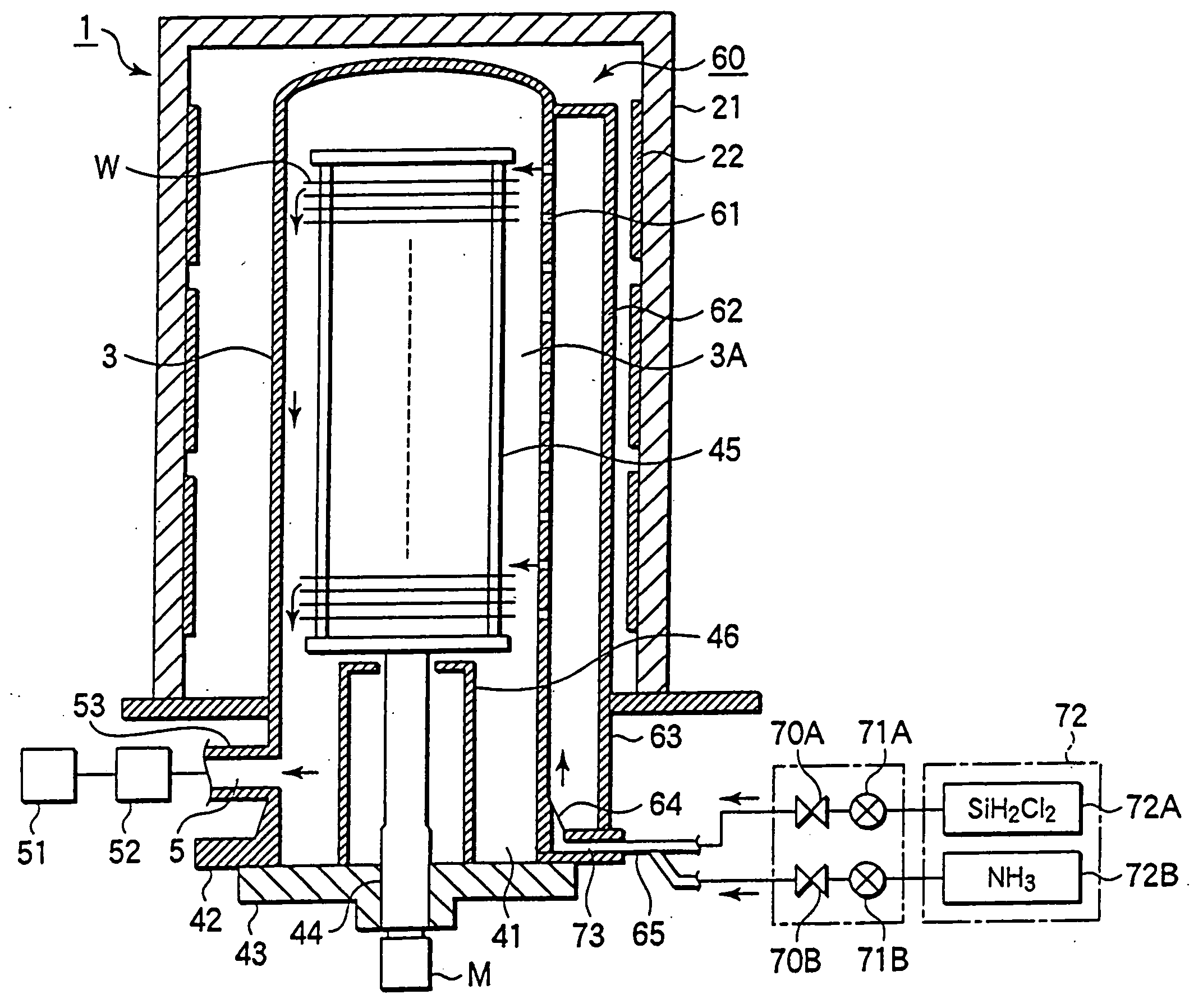
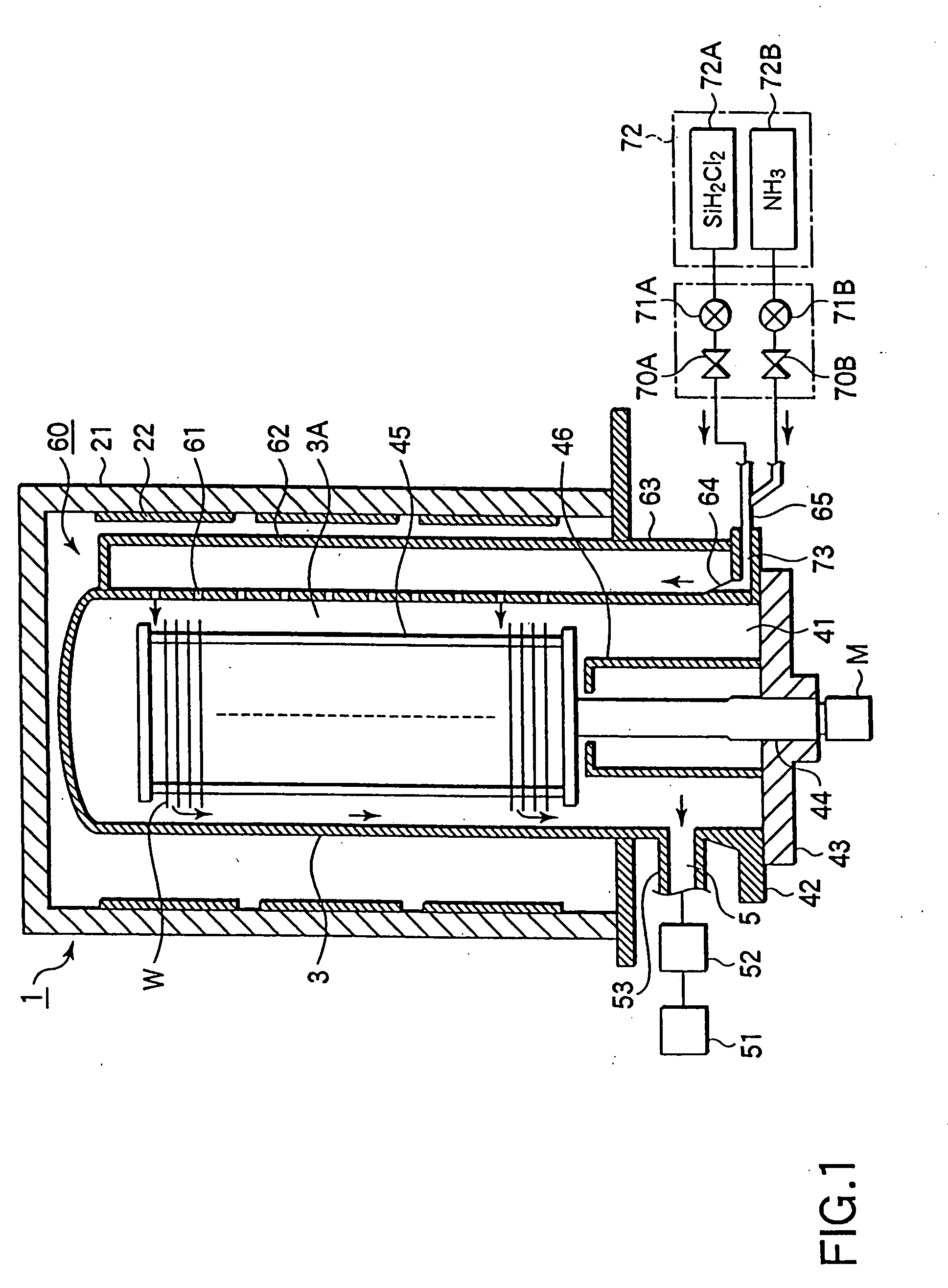
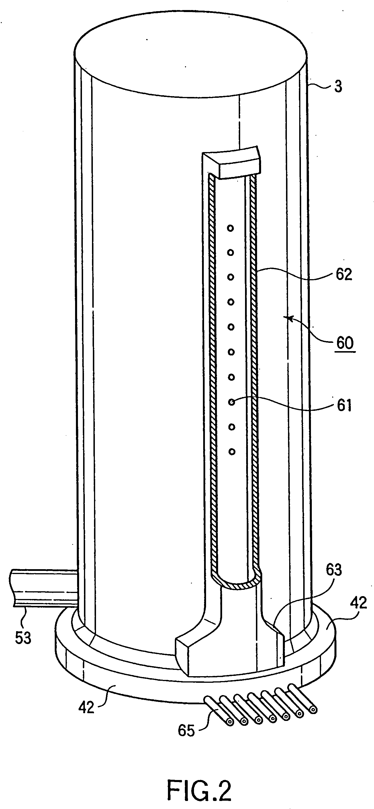
The present invention provides a heat processing apparatus for a semiconductor process that can improve the uniformity of film thickness and reduce the gap between the inner wall of a reaction tube and target substrates. The apparatus is easy to install and maintain. It includes a reaction tube with a process field for storing target substrates, a support member for supporting the substrates, an exhaust system for exhausting the interior of the process field, a heater for heating the substrates, a gas supply duct for supplying a process gas to the process field, and a gas delivery system for delivering the process gas to the process field through gas delivery holes and a gas delivery hole in the reaction tube. The gas supply duct is integrally provided outside the reaction tube and extends vertically to cover the process field. The gas delivery system is connected to the bottom of the gas supply duct to supply the process gas to the process field. The apparatus can improve the quality and efficiency of semiconductor processes.

Problems solved by technology

If the uniformity in gas flow rate among the holes is lost, it becomes difficult to form films with high uniformity among the target substrates.
Furthermore, the product deposited in the holes may be dropped by the pressure of the process gas and cause particle contamination.
Consequently, the gap between the reaction tube and the target substrates increases, and the planar uniformity of the film thickness degrades.
However, as the distance between the wall surface of the reaction tube and the outer surfaces of the target substrates is not constant, the planar uniformity of the film thickness degrades.
In this case, the cleaning time in the reaction tube prolongs, and the apparatus becomes bulky.
However, this technique requires, e.g., five or more gas supply pipes, undesirably leading to a large-scale process gas supply facility.

Method used


Image

  • Heat processing apparatus for semiconductor process
  • Heat processing apparatus for semiconductor process
  • Heat processing apparatus for semiconductor process

Examples


first embodiment

[0034]FIG. 1 is a sectional side view showing the overall arrangement of a heat processing apparatus for a semiconductor process according to the first embodiment of the present invention. This heat processing apparatus 1 has a cylindrical reaction tube 3 made of a heat-resistant insulating material, e.g., quartz, and having a circular section. The reaction tube 3 includes a process field 3A where semiconductor wafers W stacked at intervals are to be stored. The reaction tube 3 has an opening 41, serving as a transfer port, at its proximal end side (lower end side). A flange 42 integral with the reaction tube 3 is formed on the edge portion of the opening 41. The flange 42 engages with a lid 43 vertically moved by a boat elevator (not shown), so that the opening 41 can be hermetically closed.

[0035] A cylindrical cover 21 made of, e.g., a heat insulating material, surrounds the reaction tube 3. A plurality of heaters 22 are disposed along the inner wall surface of the cylindrical co...

second embodiment

[0051]FIG. 6 is a sectional side view showing the overall arrangement of a heat processing apparatus for a semiconductor process according to the second embodiment of the present invention. FIG. 7 is a partially cutaway perspective view showing a reaction tube and a gas supply duct in the heat processing apparatus in FIG. 6. In this heat processing apparatus 1X, a gas supply duct 60 and gas delivery holes 61 are arranged in the same manner as in the heat processing apparatus 1 of the first embodiment. Above the uppermost gas delivery hole 61 in the gas supply duct 60 and above a process field 3A, a pressure equalization hole 66 communicating with the interior of a reaction tube 3 is formed. The pressure equalization hole 66 is formed so that process gases are supplied to a portion above a process field in the reaction tube 3 where wafers W are held. The pressure equalization hole 66 has an opening area larger than that of each gas delivery hole 61, and forms a substantially rectangu...

third embodiment

[0054]FIG. 8 is a sectional side view showing the overall arrangement of a heat processing apparatus for a semiconductor process according to the third embodiment of the present invention. FIG. 9 is a partially cutaway perspective view showing a reaction tube and a gas supply duct in the heat processing apparatus in FIG. 8. In this heat processing apparatus 1Y, a gas supply duct 60 extends from the bottom portion to the top portion of a reaction tube 3, as shown in FIG. 9 as well. In this case, the temperature of the lower portion of a process field 3A must be set higher than that of the upper portion by separately controlling, e.g., three heaters 22 that are divided in the vertical direction, so that a temperature gradient is formed in the process field 3A in the vertical direction. Therefore, this heat process is applied to a process in which temperature difference among wafers W does not influence the yield. An example of such a heat process includes a process of forming an SiO2 ...


PUM

PropertyMeasurementUnit
diametersaaaaaaaaaa
diameteraaaaaaaaaa
pressureaaaaaaaaaa

Abstract

A heat processing apparatus for a semiconductor process includes a reaction tube including a process field configured to store a plurality of target substrates stacked at intervals. A gas supply duct is integrally provided outside the wall of the reaction tube to extend vertically in a range that covers the process field. A plurality of gas delivery holes are formed in the side portion of the wall of the reaction tube, to be vertically arrayed in a range that covers the process field and communicate with the gas supply duct. A gas supply system is connected to a bottom portion of the gas supply duct to supply a process gas to the process field through the gas supply duct and the plurality of gas delivery holes.

Description

BACKGROUND OF THE INVENTION [0001] 1. Field of the Invention [0002] The present invention relates to a heat processing apparatus for a semiconductor process for forming a film on a target substrate such as a semiconductor wafer. The semiconductor process refers to various types of processes which are performed to form a semiconductor layer, an insulating layer, a conductive layer, or the like in a predetermined pattern on a target substrate such as a semiconductor wafer or a glass substrate for an FPD (Flat Panel Display), such as an LCD (Liquid Crystal Display), thereby manufacturing a structure including a semiconductor device, a wiring line connected to the semiconductor device, an electrode, or the like on the target substrate. [0003] 2. Description of the Related Art [0004] Examples of a semiconductor manufacturing apparatus include a batch type heat processing apparatus such as a vertical furnace or a horizontal furnace. A vertical heat processing apparatus (vertical furnace) ...

Claims


Application Information

Patent Timeline
Patent Type & Authority Applications(United States)
IPC IPC(8): C23C16/00
CPCC23C16/45578C23C16/345C23C16/46
Inventor INOUE, HISASHIENDO, ATSUSHI
Owner TOKYO ELECTRON LTD
Learn More