Sub-lithographic local interconnects, and methods for forming same

a local interconnect and sublithographic technology, applied in the field of sublithographic local interconnects and methods for forming same, can solve the problems of difficult scaling of sram cells, limited scaling effort overlay limits of conventional lithographic printing, so as to achieve further scaling of sram cell layout, the effect of significantly reducing the number of metal contacts and metal interconnects in each sram cell

Inactive Publication Date: 2008-04-10
IBM CORP
View PDF4 Cites 107 Cited by
  • Summary
  • Abstract
  • Description
  • Claims
  • Application Information

AI Technical Summary

Benefits of technology

[0009]The present invention solves the above-described problems by providing improved SRAM structures, each of which contains two sub-lithographic interconnects that replace the four metal contacts at the contact level and the two local interconnects at the M1 level fo

Problems solved by technology

However, the scaling effort is significantly limited by conventional lithographic printing, which has been used for patterning the metal contacts and the metal interconnects of the SRAM cells.
Due to the large number of metal contacts at the CA level and meta

Method used


Image

  • Sub-lithographic local interconnects, and methods for forming same
  • Sub-lithographic local interconnects, and methods for forming same
  • Sub-lithographic local interconnects, and methods for forming same

Examples


Embodiment Construction

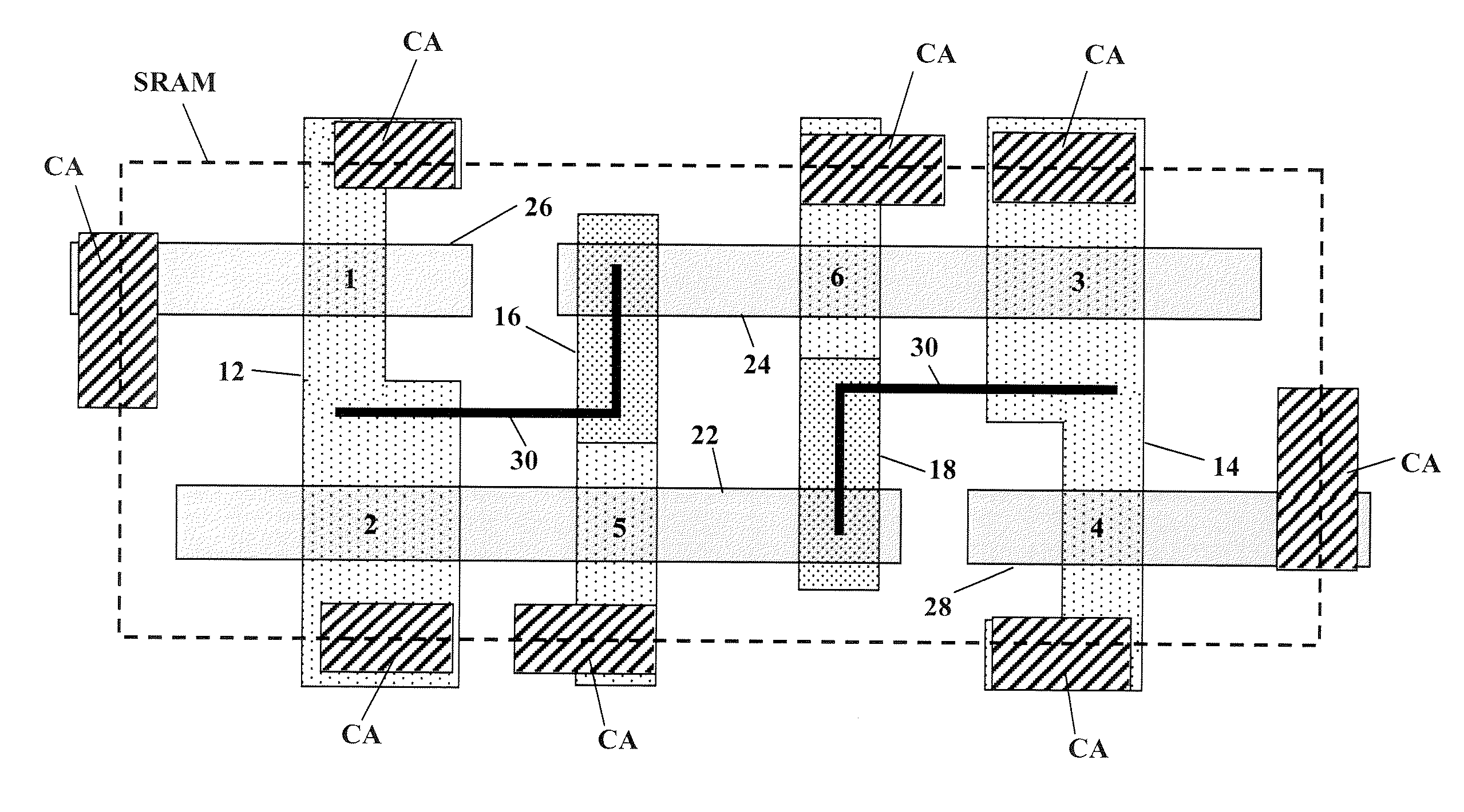
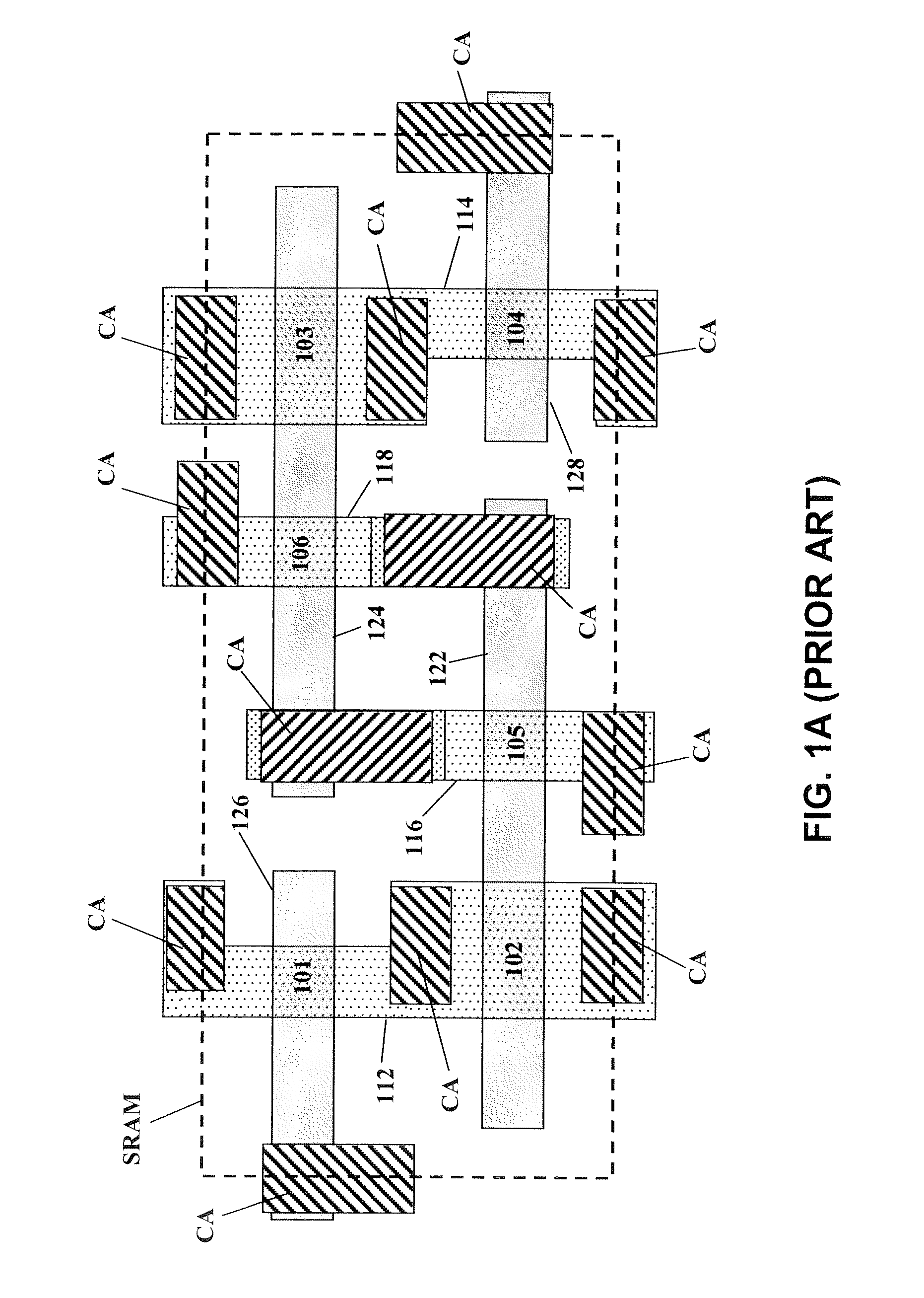
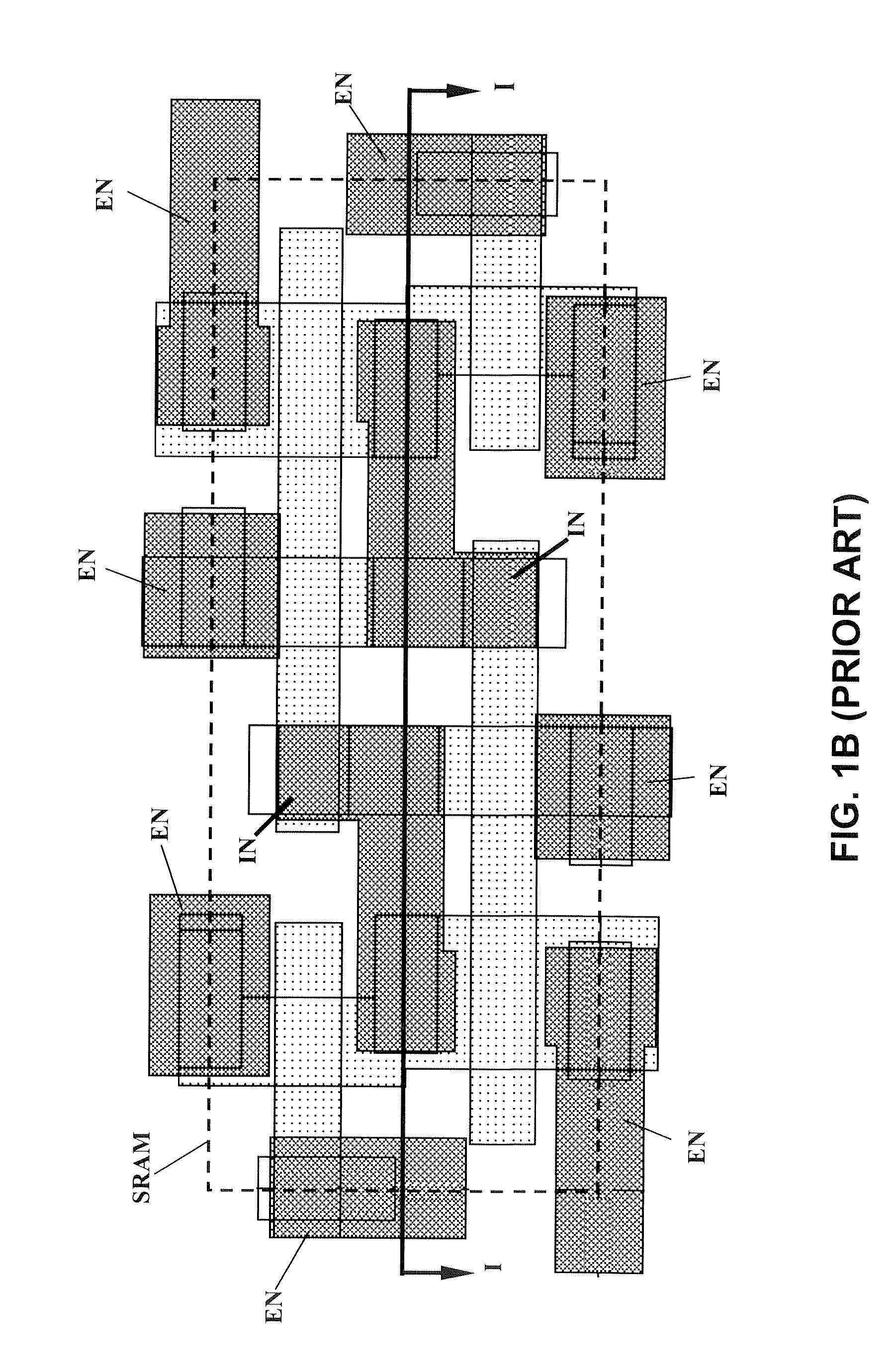
[0040]In the following description, numerous specific details are set forth, such as particular structures, components, materials, dimensions, processing steps and techniques, in order to provide a thorough understanding of the present invention. However, it will be appreciated by one of ordinary skill in the art that the invention may be practiced without these specific details. In other instances, well-known structures or processing steps have not been described in detail in order to avoid obscuring the invention.

[0041]It will be understood that when an element as a layer, region or substrate is referred to as being “on” or “over” another element, it can be directly on the other element or intervening elements may also be present. In contrast, when an element is referred to as being “directly on” or “directly over” another element, there are no intervening elements present. It will also be understood that when an element is referred to as being “beneath” or “under” another element...


PUM


Abstract

The present invention relates to a semiconductor device having first and second active device regions that are located in a semiconductor substrate and are isolated from each other by an isolation region therebetween, while the semiconductor device contains a first sub-lithographic interconnect structure having a width ranging from about 20 nm to about 40 nm for connecting the first active device region with the second active device region. The semiconductor device preferably contains at least one static random access memory (SRAM) cell located in the semiconductor substrate, and the first sub-lithographic interconnect structure directly cross-connects a pull-down transistor of the SRAM cell with a pull-up transistor thereof without any metal contact therebetween. The first sub-lithographic interconnect structure can be readily formed by lithographic patterning of a mask layer, followed by formation of sub-lithographic features using either self-assembling block copolymers or dielectric sidewall spacers.

Description

FIELD OF THE INVENTION[0001]This invention relates to semiconductor devices that comprise local conductive interconnects having sub-lithographic widths. More specifically, the present invention relates to sub-45 nm or sub-32 nm static random access memory (SRAM) cells with local conductive interconnects having sub-lithographic widths, as well as methods for fabricating such SRAM cells.BACKGROUND OF THE INVENTION[0002]A static random access memory (SRAM) is a significant memory device due to its high speed, low power consumption, and simple operation. Unlike a dynamic random access memory (DRAM) cell, the SRAM does not need to regularly refresh the stored data and it has a straightforward design.[0003]Each bit in a typical six-transistor SRAM (6T-SRAM) cell is stored on four transistors, generally referred to as load transistors (or pull-up transistors) and driver transistors (or pull-down transistors), that form a flip-flop circuit containing two cross-coupled inverters. This storag...

Claims


Application Information

Patent Timeline
IPC IPC(8): H01L23/52
CPCB82Y10/00H01L21/0338H01L21/31144H01L27/1104H01L21/76895H01L27/11H01L21/76816H01L23/485H10B10/00H10B10/12
Inventor YANG, HAININGMANDELMAN, JACK A.LI, WAI-KIN
Owner IBM CORP
Why Eureka
Try Eureka