Polishing tool and polishing method and apparatus using same

Inactive Publication Date: 2008-04-10
DISCO CORP
View PDF11 Cites 7 Cited by
  • Summary
  • Abstract
  • Description
  • Claims
  • Application Information

AI Technical Summary

Benefits of technology

[0004] An object of the present invention is to provide a new and improved polishing tool which polishes a back side of a semiconductor wafer with a high polishing efficiency and a high polishing quali

Problems solved by technology

When the back side of the semiconductor wafer is ground by such a grinding method, so-called processing distortion is generated in the back side of the semiconductor wafer, thereby decreasing transverse rupture strength considerably.
Polishing using free abrasive grains, however, involves the problems that the supply, recovery, etc. of the free abrasive grains require tiresome procedure, leading to a low efficie

Method used


Image

  • Polishing tool and polishing method and apparatus using same
  • Polishing tool and polishing method and apparatus using same
  • Polishing tool and polishing method and apparatus using same

Examples


Embodiment Construction

[0047] Embodiments of the present invention will be described in further detail by reference to the accompanying drawings.

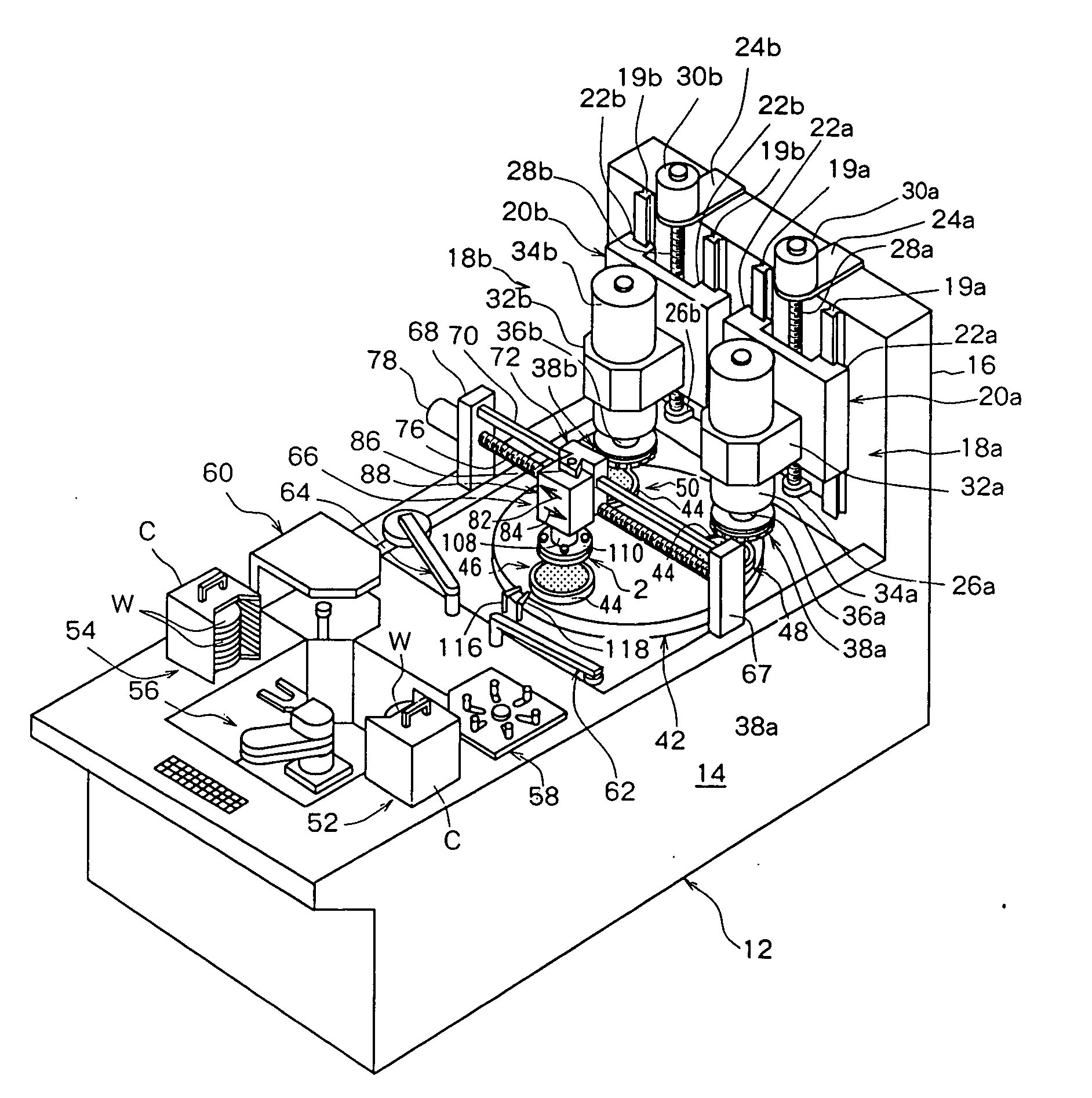
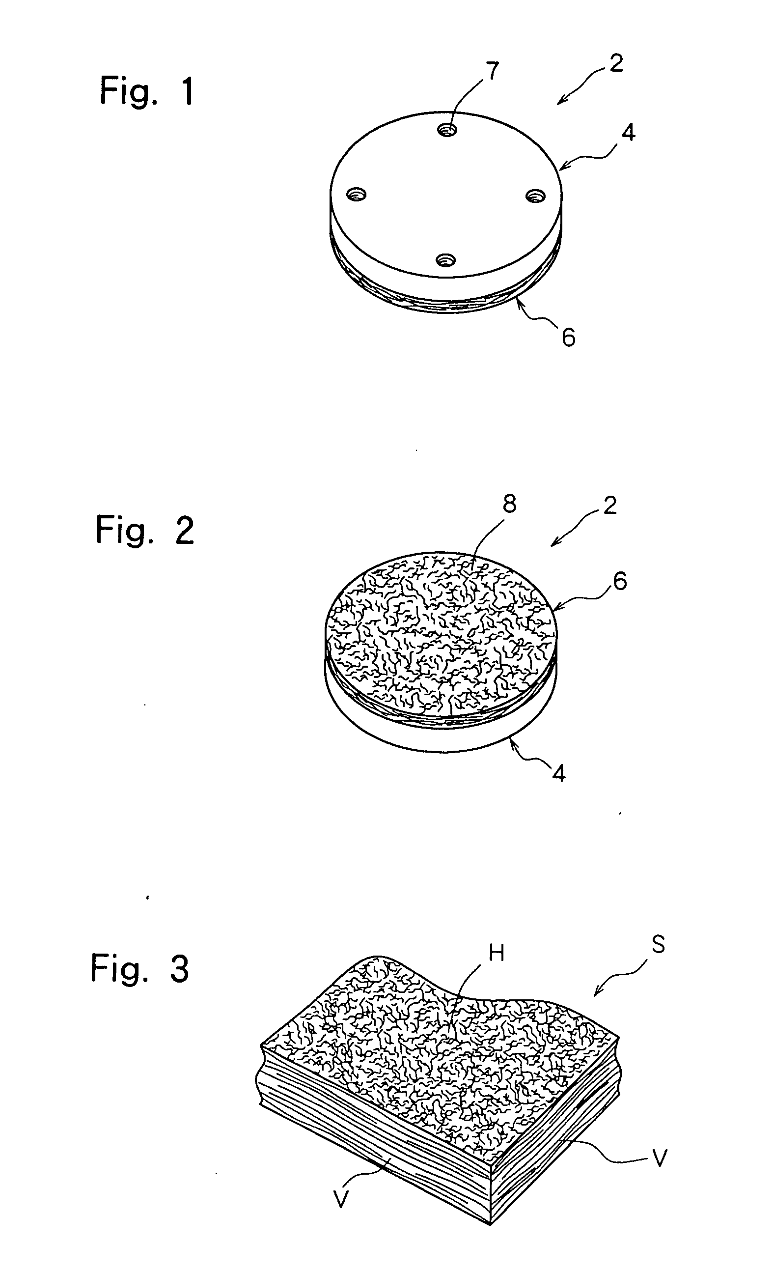
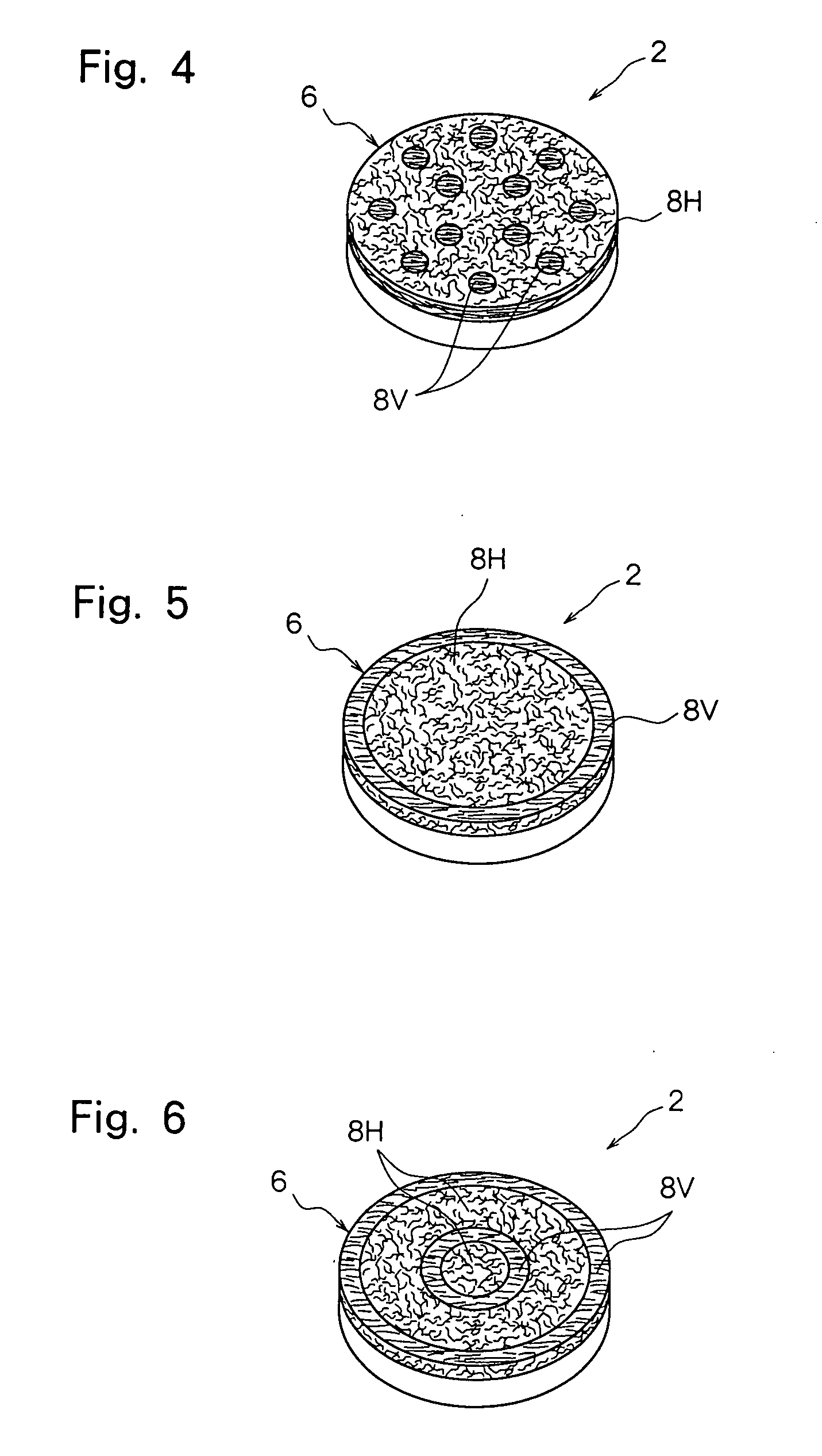
[0048]FIGS. 1 and 2 show a preferred embodiment of a polishing tool constructed in accordance with the present invention. The illustrated polishing tool, shown entirely by a numeral 2, is composed of a support member 4 and polishing means 6. The support member 4 is advantageously formed from a suitable metal such as aluminum, is disc-shaped, and has a flat circular support surface, namely, a lower surface. As shown in FIG. 1, a plurality of (four in the drawings) tapped blind holes 7, extending downward from an upper surface of the support member 4, are formed at circumferentially spaced locations in the support member 4. The polishing means 6 is also disc-shaped, and the outer diameter of the support member 4 and the outer diameter of the polishing means 6 are substantially the same. The polishing means 6 is bonded to the lower surface of the support member 4 (...


PUM

PropertyMeasurementUnit
Timeaaaaaaaaaa
Percent by massaaaaaaaaaa
Densityaaaaaaaaaa

Abstract

A polishing tool comprising a support member, and polishing means fixed to the support member. The polishing means is composed of felt having a density of 0.20 g/cm3 or more and a hardness of 30 or more, and abrasive grains dispersed in the felt. A polishing method and apparatus involving pressing the polishing means against a surface of a workpiece to be polished, while rotating the workpiece and also rotating the polishing tool.

Description

FIELD OF THE INVENTION [0001] This invention relates to a polishing tool, especially a polishing tool suitable for polishing a back side of a semiconductor wafer having processing distortion, and a polishing method and apparatus using such a polishing tool. DESCRIPTION OF THE PRIOR ART [0002] In a process for manufacturing semiconductor chips, many rectangular areas are demarcated by streets arranged in a lattice pattern on a face side of a semiconductor wafer, and semiconductor circuits are disposed in the respective rectangular areas. The semiconductor wafer is divided along the streets to convert the rectangular areas into semiconductor chips. To make the semiconductor chips compact and lightweight, it is often desired to grind a back side of the semiconductor wafer before separation of the rectangular areas into individual chips, thereby decreasing the thickness of the semiconductor wafer. Grinding of the back side of the semiconductor wafer is usually performed by pressing grin...

Claims


Application Information

Patent Timeline
IPC IPC(8): B24B29/02B24B7/22B24D11/00B24D13/14H01L21/306
CPCB24B7/228B24D13/147B24D11/00
Inventor SEKIYA, SINNOSUKEYAMAMOTO, SETSUOKOMA, YUTAKAAOKI, MASASHIMATSUYA, NAOHIRO
Owner DISCO CORP
Why Eureka
Try Eureka