Quartz Jig and Semiconductor Manufacturing Apparatus

a semiconductor and manufacturing apparatus technology, applied in the direction of chemically reactive gases, coatings, crystal growth processes, etc., can solve the problems of unable to achieve target process conditions, affecting the quality of semiconductor products, etc., to suppress the pollution of wafers and keep them.

Inactive Publication Date: 2008-04-24
SHIN-ETSU HANDOTAI CO LTD
View PDF6 Cites 154 Cited by
  • Summary
  • Abstract
  • Description
  • Claims
  • Application Information

AI Technical Summary

Benefits of technology

[0022] This quartz jig is composed of a transparent quartz specifically in the portion thereof brought into contact with the soaking jig, where the silicon by-product tends to grow most rapidly. The transparent quartz is more dense as compared with the opaque quartz, and has almost no voids contained therein, and can thereby largely suppress any possibility of releasing, together with the silicon by-product, of quartz composing the surficial portion of the jig, and any possibility of dusting, in a particle form, of fine quartz between the voids as a result of exposure to the etching gas for removing the silicon by-product.
[0023] Next, the quartz jig of this invention preferably has a core portion composed of an opaque quartz, and a surficial portion composed of a transparent quartz, and covers the core portion so as to prevent the surface thereof from being exposed. This configuration is effective not only in that the effects described in the above can be obtained over the entire surface of the quartz jig by virtue of the transparent quartz (surficial portion), but also in that the soaking jig can be more readily kept at a desired temperature, because the opaque quartz (core portion) which lies under the transparent quartz (surficial portion) reflects infrared radiation or the like, even if heat release by the infrared radiation or the like occurs from the soaking jig.
[0024] Next, the quartz jig of this invention may have a geometry such as being notched in a portion which overlaps a transfer path of a semiconductor wafer loaded to and unloaded from the semiconductor manufacturing apparatus. Because no quartz jig

Problems solved by technology

Adhesion of the particles onto the main surface of the wafer may induce crystal defects in the epitaxial layer.
On the other hand, the silicon by-product grown on the inner wall of the quartz chamber 6 may alter heat conductivity of the quartz chamber 6, and may make it impossible to achieve target process conditions, raising a need of periodical removal of the silicon by-product.
The etching gas used herein, however, etches also the various components in the quartz chamber 6, such as the soaking jig 3, the quartz jig 4, the chamber top plate 6a and the chamber side wall 6c, and consequently degrades these components over a long period of use.
Once the voids are exposed as a result of degradation, a large amount of quartz between the voids is released by the etching, raising a cause of particle pollution.
In this configuration, however, the nozzle base portion composed of the opaque quartz is exposed to the etching gas, and therefore cannot be prevented from degrading, even if the silicon by-product could be etched.
Sand blasting accomplished by blasting quartz powder against the quartz jig may, however, result in adhesion of the quartz powder onto the quartz jig.
Thus-adhered quartz powder may delaminate from the quartz jig due to expansion and shrinkage of the quartz jig cau

Method used


Image

  • Quartz Jig and Semiconductor Manufacturing Apparatus
  • Quartz Jig and Semiconductor Manufacturing Apparatus
  • Quartz Jig and Semiconductor Manufacturing Apparatus

Examples


example 1

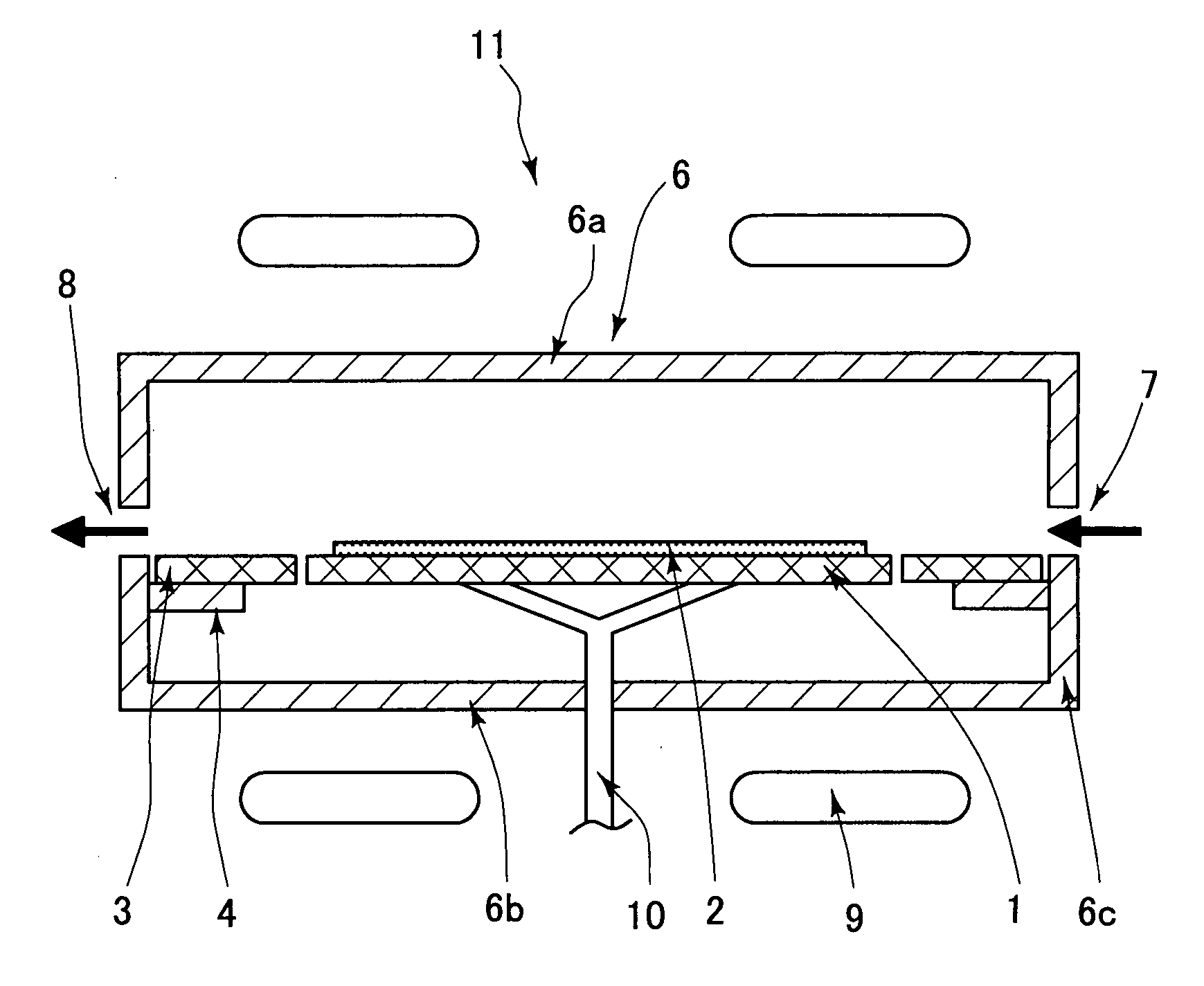
[0050] A silicon single crystal wafer of a p-conductivity type, 200 mm in diameter and with a crystal orientation was prepared, and loaded into the single-wafer-processing-type CVD apparatus as shown in FIG. 1. A quartz jig used herein in the CVD apparatus was the ring-form jig (see FIG. 2) composed of the opaque quartz, having on the surface thereof, which is brought into contact with the soaking jig, the transparent quartz of 1 mm thick fused therewith. The silicon single crystal wafer loaded into the CVD apparatus was heated to 1,050° C., hydrogen-diluted trichlorosilane as the source gas was introduced into the quartz chamber, and thereby a silicon epitaxial layer of 6 μm thick was grown on the main surface of the wafer. This process was repeated 10 times, and dry etching of the interior of the CVD apparatus was carried out using hydrochloric acid gas. Processing of 10 silicon wafers and a single time of dry etching were carried out in a successive manner.

example 2

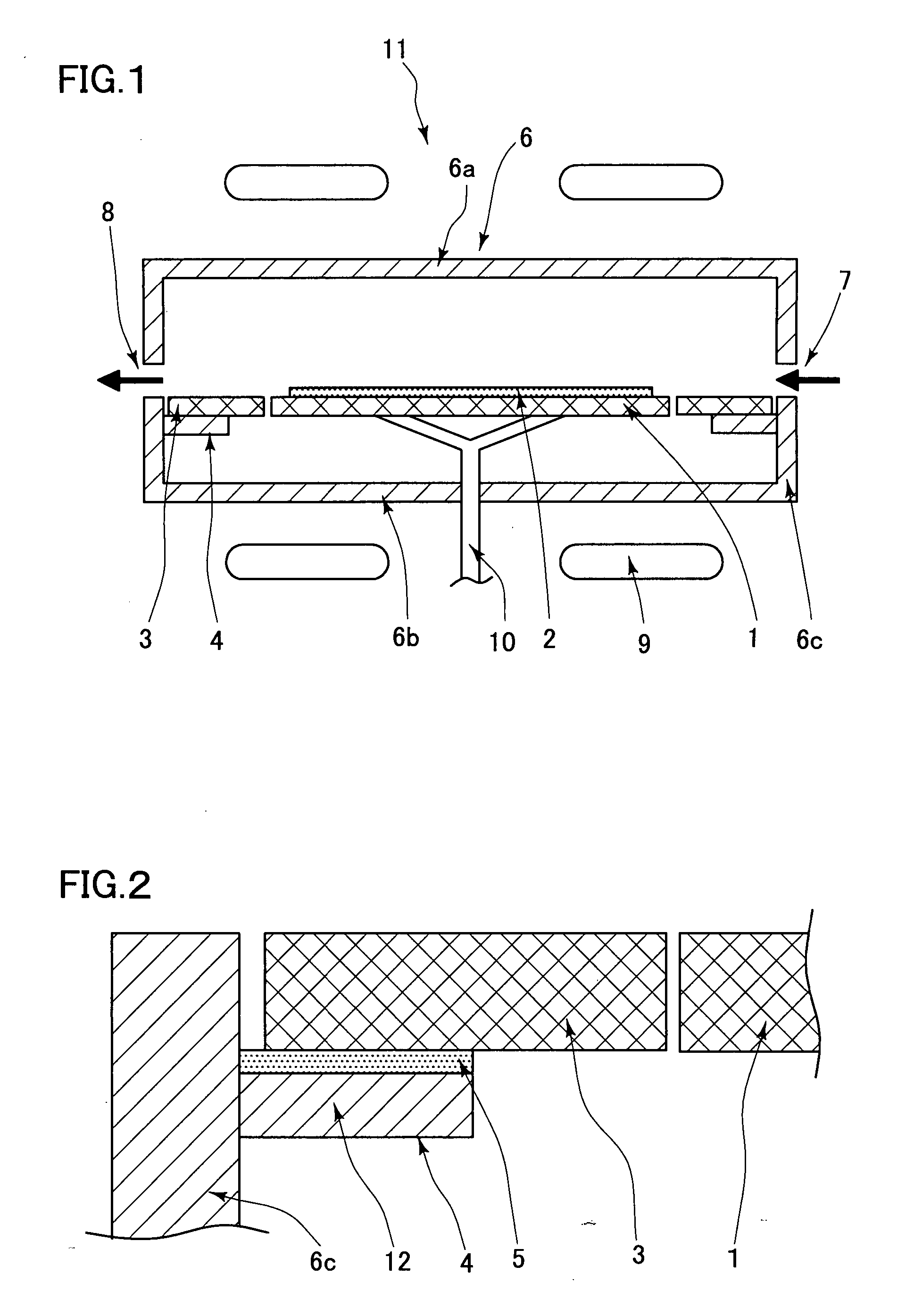
[0051] A silicon single crystal wafer same as that described in Example 1 was prepared, and a silicon epitaxial layer was grown to as thick as 6 μm on the main surface of the wafer under same conditions. The quartz jig used herein in the CVD apparatus was a ring-form jig (see FIG. 3) composed of the opaque quartz, having on the entire surface thereof the transparent quartz of 1 mm thick fused therewith.

example 3

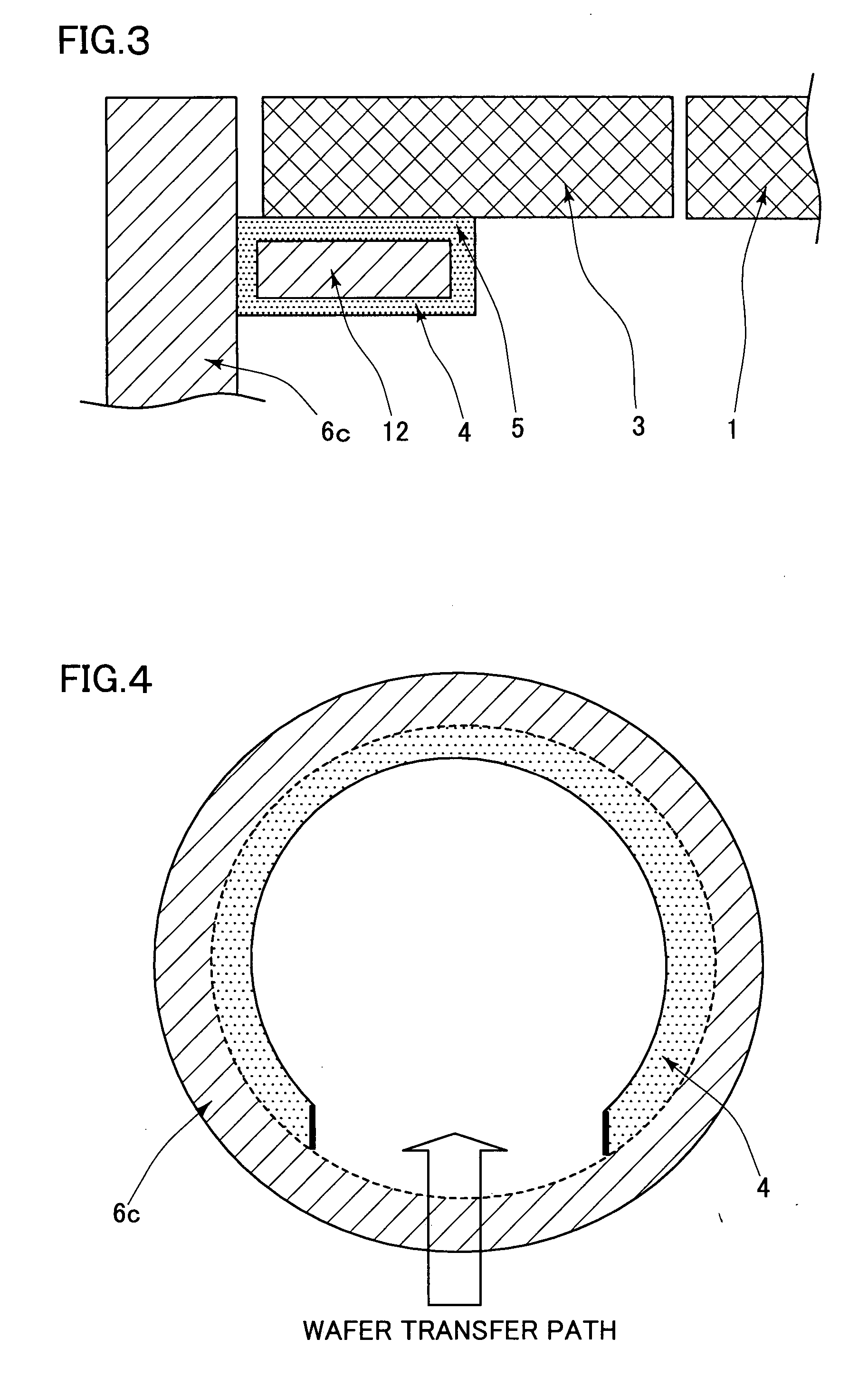
[0052] A silicon single crystal wafer same as that described in Example 1 was prepared, and a silicon epitaxial layer was grown to as thick as 6 μm on the main surface of the wafer under same conditions. The quartz jig used herein was a jig (see FIG. 4) composed of the opaque quartz, having on the surface thereof, which is brought into contact with the soaking jig, the transparent quartz of 1 mm thick fused therewith, and notched in a portion thereof which overlaps a transfer path of the wafer.


PUM

PropertyMeasurementUnit
Temperatureaaaaaaaaaa
Heightaaaaaaaaaa
Transparencyaaaaaaaaaa

Abstract

A quartz jig of this invention is such as being provided inside a semiconductor manufacturing apparatus allowing therein growth of an epitaxial layer on a main surface of a semiconductor wafer, capable of supporting a soaking jig which keeps, during epitaxial growth, uniform temperature of a susceptor allowing thereon placement of the semiconductor wafer, and has the top surface thereof aligned almost at the same level of height with the top surface of the susceptor, and is characterized as being composed of transparent quartz at least in a portion thereof brought into contact with the soaking jig. This configuration successfully provides a quartz jig supporting the soaking jig in the semiconductor manufacturing apparatus while suppressing generation of particles, and a semiconductor manufacturing apparatus provided with this sort of quartz jig.

Description

RELATED APPLICATIONS [0001] This application claims the priorities of Japanese Patent Application No. 2004-243722 filed on Aug. 24, 2004, which is incorporated herein by reference. BACKGROUND OF THE INVENTION [0002] 1. Field of the Invention [0003] This invention relates to a quartz jig provided inside a semiconductor manufacturing apparatus allowing therein growth of an epitaxial layer on a main surface of a semiconductor wafer, capable of supporting a soaking jig which keeps, during epitaxial growth, uniform temperature of a susceptor allowing thereon placement of the semiconductor wafer, and has the top surface thereof aligned almost at the same level of height with the top surface of the susceptor, and a semiconductor manufacturing apparatus provided with the quartz jig. [0004] 2. Description of the Related Art [0005] As a semiconductor manufacturing apparatus used for manufacturing silicon epitaxial wafers and semiconductor devices, having conventionally been used, for example,...

Claims


Application Information

Patent Timeline
IPC IPC(8): C23C16/00
CPCC23C16/4583C30B25/10H01L21/68757H01L21/00H01L21/67115C30B25/12H01L21/683H01L21/687
Inventor OTSUKA, TORUKANNO, TAKAO
Owner SHIN-ETSU HANDOTAI CO LTD
Why Eureka
Try Eureka