Wireless Chip

a wireless chip and chip technology, applied in the direction of electrical equipment, support structure mounting, semiconductor devices, etc., can solve the problems of less easily received with a smaller antenna and shorter communication distance, and achieve the effect of improving communication distan

Inactive Publication Date: 2008-04-24
SEMICON ENERGY LAB CO LTD
View PDF3 Cites 33 Cited by
  • Summary
  • Abstract
  • Description
  • Claims
  • Application Information

AI Technical Summary

Benefits of technology

[0011] In view of the foregoing problems, a power source circuit of an ID chip of the invention generates a higher power source voltage than a power source voltage generated in a conventional ID chip. As a result, the communication distance can be improved. That is, the invention realizes a configuration where internal circuits of an ID chip can operate stably even when a signal amplitude obtained from an antenna circuit is small in order to improve the communication distance of the ID chip.
[0020] A boosting power source circuit of the invention can operate normally and generate a power source voltage which is high enough to operate a logic circuit even in the case where a signal amplitude large enough to operate the logic circuit is not obtained with a conventional power source circuit. As a result, a more compact ID chip having an improved communicable distance can be realized.

Problems solved by technology

On the other hand, it is less easily received with a smaller antenna, thereby the communication distance becomes shorter.

Method used


Image

  • Wireless Chip
  • Wireless Chip
  • Wireless Chip

Examples


embodiment mode 1

[0045] In this embodiment mode, a configuration of an ID chip of the invention is described.

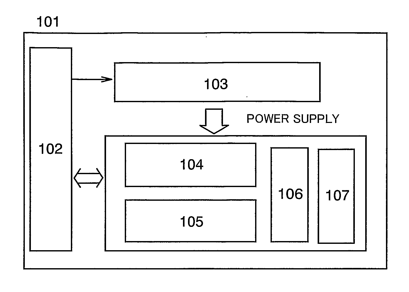
[0046] As shown in FIG. 1, an ID chip 101 includes an antenna circuit 102, a boosting power source circuit 103, a demodulation circuit 104, a modulation circuit 105, a memory interface (IF) 106 and a memory 107. Such IC chip 101 reads or writes data from / to the memory 107 in accordance with an instruction (signal) received by the antenna circuit 102. The boosting power source circuit 103 has a function to generate a boosted power source voltage based on an AC signal generated in the antenna circuit 102, and supply power to the demodulation circuit 104, the modulation circuit 105, the memory interface (IF) 106, the memory 107 and the like.

[0047] The boosting power source circuit 103 of the invention can, even in the case where a signal amplitude large enough to operate an internal logic circuit of a demodulation circuit or a modulation circuit cannot be obtained, operate normally and generat...

embodiment mode 2

[0065] Description is made on a specific circuit configuration of the boosting power source circuit of the invention.

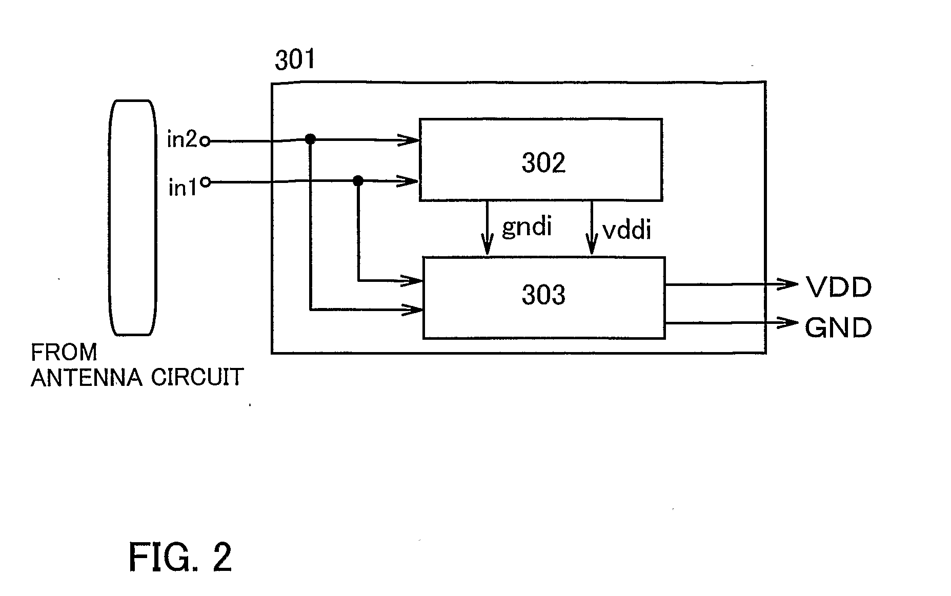
[0066] A boosting power source circuit 501 shown in FIG. 4 includes a rectifier circuit 502 and a boosting circuit 503, and input terminals in1 and in2 thereof receive signals from an antenna circuit directly or through capacitors. The boosting power source circuit 501 outputs a power source potential (VDD) and a ground potential (GND).

[0067] The rectifier circuit 502 includes two diodes 507 and 508 connected in series and a capacitor 506. An input terminal of the diode 507 is connected to the input terminal in1 while an output terminal thereof (node n3) is connected to one terminal of the capacitor 506 and an input terminal of the diode 508. The other terminal of the capacitor 506 is connected to the input terminal in2. Upon input of signals to the rectifier circuit 502 from the input terminals in1 and in2, the potential vddi and the potential gndi are generated. T...

embodiment 1

[0082] In this embodiment, description is made with reference to FIG. 6 on the case where a limiter circuit is provided at the output of the boosting power source circuit of the invention.

[0083] An amplitude of an input signal of an ID chip is dependent on the communication distance and the intensity of a signal source. A power source potential generated by a boosting power source circuit is dependent on the amplitude and frequency of the input signal, the number of boosting stages of the boosting power source circuit and the threshold voltage of a diode. As a result, the power source potential generated by the boosting power source circuit is dependent on the communication distance and the intensity of a signal source.

[0084] The boosting circuit of the invention operates with high performance even in the case where an amplitude of an input signal is small. Meanwhile, in the case where an amplitude of an input signal is large, there is a possibility that an extremely high power so...


PUM


Abstract

The size of a wireless chip is often determined according to an antenna circuit thereof. Power source voltage or power supplied to the wireless chip can be more easily received with a larger antenna. On the other hand, there has been an increasing demand for a compact wireless chip, and it is thus necessary to downsize an antenna. In view of this, the invention provides a wireless chip capable of data communication with a small antenna, namely a compact wireless chip having an improved communicable distance. A power source circuit of an ID chip of the invention generates a higher power source voltage than a power source voltage generated in a conventional ID chip, by using a boosting power source circuit having a boosting circuit and a rectifier circuit.

Description

TECHNICAL FIELD [0001] The present invention relates to a wireless chip and a manufacturing method thereof. BACKGROUND ART [0002] In recent years, wireless chips for wireless data transmission / reception are actively developed. The wireless chip for data transmission / reception is called an IC chip, an RF tag, an RFID, a wireless tag, an electronic tag, a wireless processor, a wireless memory and the like, and most of the wireless chips which are currently in practical use are formed using a silicon substrate. [0003] Such a wireless chip is attracting attention as an alternative to a barcode having a small amount of data so as to be used for merchandise management (see Patent Document 1). In addition, a contactless IC card having a high security function is also attracting attention in order to prevent the counterfeiting or unauthorized use. [0004]FIG. 23 shows an example of a conventional configuration of such a wireless chip. Shown in FIG. 23 is a wireless chip which reads and write...

Claims


Application Information

Patent Timeline
Patent Type & Authority Applications(United States)
IPC IPC(8): H02J17/00
CPCH01L27/1214H01L29/78648H01L27/13H01L27/1266
Inventor KATO, KIYOSHI
Owner SEMICON ENERGY LAB CO LTD
Why Eureka
Try Eureka