Optical modulator utilizing multi-level signaling

a multi-level signaling and optical modulator technology, applied in optics, instruments, electrical equipment, etc., can solve the problems of increasing the data rate being transmitted over the fiber(s), not being able to use lithium niobate-based optical devices in such situations, and the dynamic behavior of the laser itself introduces distortion. , to achieve the effect of reducing the serial symbol ra

Inactive Publication Date: 2008-04-24
CISCO TECH INC
View PDF13 Cites 42 Cited by
  • Summary
  • Abstract
  • Description
  • Claims
  • Application Information

AI Technical Summary

Benefits of technology

[0008]The need remaining in the art is addressed by the present invention which relates to an optical modulator and, more particularly, to an optical modulator including multiple sections of different lengths so as to transmit multiple data bits at a time, reducing the serial symbol rate.
[0012]Advantageously, the use of multiple electrodes of different lengths to perform multi-level signaling has been found to reduce the logic associated applying the various input signals to the multiple electrodes. Indeed, it has been found that the transmitted symbol rate can be twice as fast as transmitting the original data.

Problems solved by technology

The disadvantage of this method is that when higher switching speeds are required, the dynamic behavior of the semiconductor material of the laser itself introduces distortion, primarily in the form of chirp.
Clearly, the use of lithium niobate-based optical devices in such a situation is not an option.
However, this aggregation results in increasing the data rate being transmitted over the fiber(s).
The inherent bandwidth limitation of the fiber associated with dispersion effects limits the distance an optical signal may propagate at this rate.

Method used


Image

  • Optical modulator utilizing multi-level signaling
  • Optical modulator utilizing multi-level signaling
  • Optical modulator utilizing multi-level signaling

Examples


Embodiment Construction

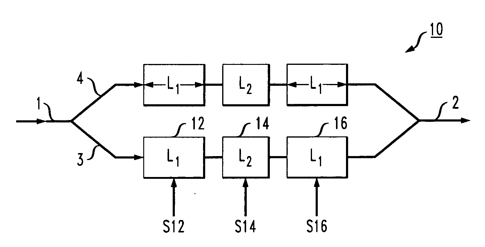
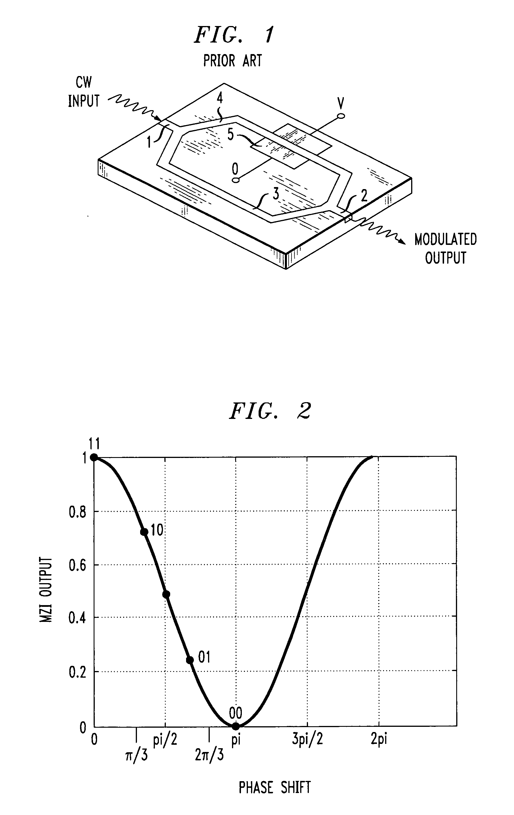
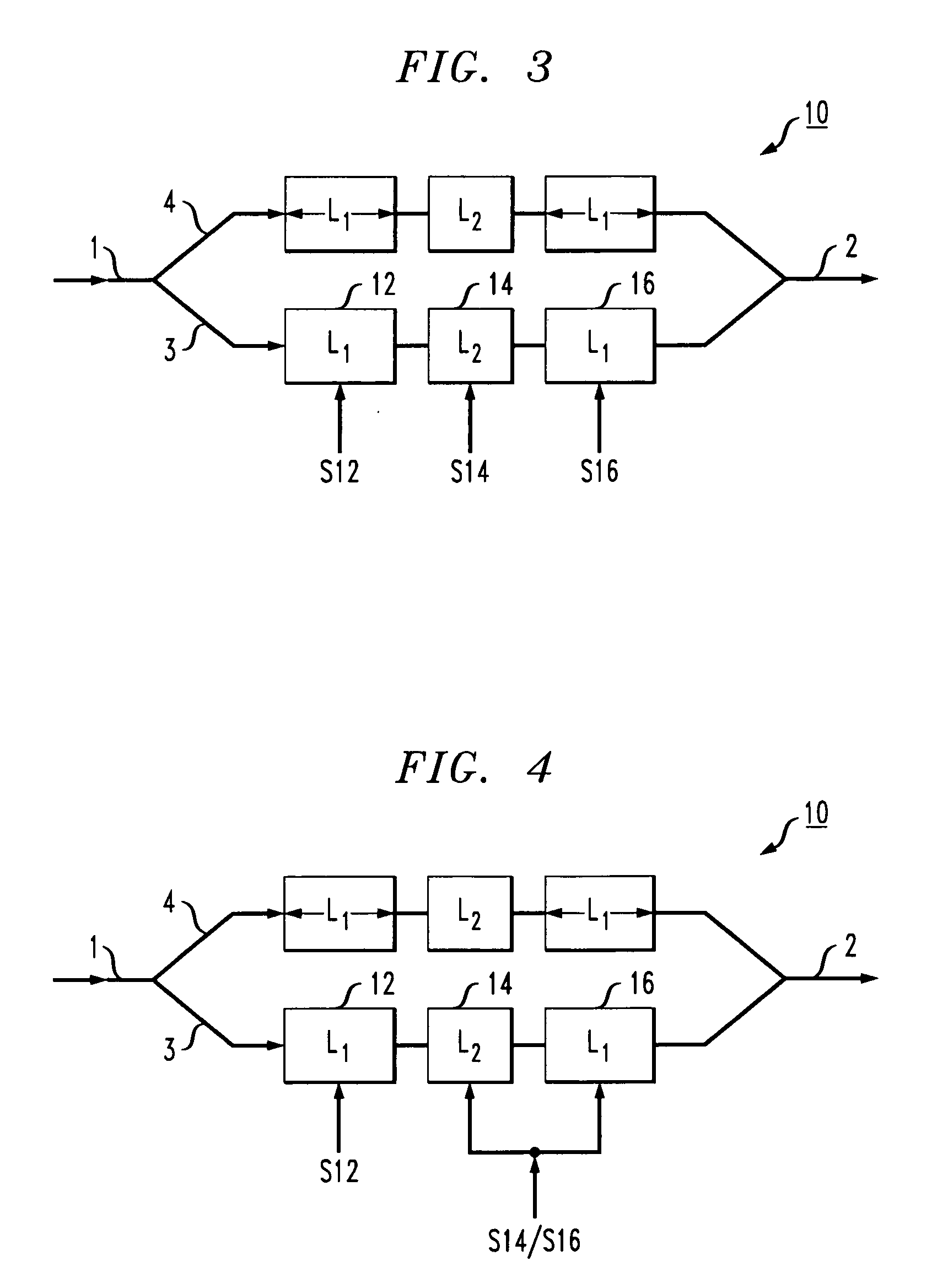
[0020]FIG. 1 illustrates an exemplary prior art Mach-Zehnder modulator that may be re-configured as described below to provide multi-level data transmission in accordance with the present invention. As shown, the prior art modulator comprises an input waveguide section 1 and an output waveguide section 2. A pair of waveguiding modulator arms 3 and 4 are shown and may be formed in one embodiment (i.e., an SOI-based embodiment) to include a capacitor-like structure.

[0021]In operation, an incoming continuous wave (CW) light signal from a laser source (not shown) is coupled into input waveguide section 1. The CW signal is thereafter split into a pair of waveguide arms 3 and 4. The application of an electrical drive signal to this modulator arm (or arms) will provide the desired phase shift to modulate the optical signal, forming a modulated optical output signal along output waveguide 2. A pair of electrodes 5 are illustrated in association with modulator arm 4 and used to provide the e...


PUM

PropertyMeasurementUnit
lengthaaaaaaaaaa
lengthsaaaaaaaaaa
phaseaaaaaaaaaa

Abstract

An optical modulator is formed to include a plurality of separate electrodes disposed along one arm, the electrodes having different lengths and driven with different signals to provide for multi-level signaling (e.g., PAM-4 signaling). By using separate drivers to energize the different sections, the number of sections energized at a given point in time will define the net phase shift introduced to the optical signal. The total length of the combined modulator sections is associated with a π phase shift (180°). Each section is driven by either a digital “one” or “zero”, so as to create the multi-level modulation. An essentially equal change in power between adjacent transmitted symbols is accomplished by properly adjusting the lengths of each individual section.

Description

CROSS-REFERENCE TO RELATED APPLICATION[0001]This application claims the benefit of U.S. Application No. 60 / 852,757, filed Oct. 19, 2006.TECHNICAL FIELD[0002]The present invention is directed to an optical modulator and, more particularly, to an optical modulator including multiple sections of different lengths so as to transmit multiple data bits at a time, reducing the serial symbol rate.BACKGROUND OF THE INVENTION[0003]Optical transmission systems are generally based on one of two methods of modulation of an optical signal, either direct modulation or external modulation. In the first of these methods, a DC current is applied to a laser, with a modulation current superimposed thereon, turning the laser “on” and “off”. The disadvantage of this method is that when higher switching speeds are required, the dynamic behavior of the semiconductor material of the laser itself introduces distortion, primarily in the form of chirp. External modulation of an optical signal produces a modula...

Claims


Application Information

Patent Timeline
Patent Type & Authority Applications(United States)
IPC IPC(8): G02F1/035
CPCG02F1/2255G02F1/0123H04B10/541
Inventor SHASTRI, KALPENDUDAMA, BIPIN
Owner CISCO TECH INC
Why Eureka
Try Eureka