
Slurry composition for forming tungsten pattern and method for manufacturing semiconductor device using the same

a technology of tungsten pattern and slurry composition, which is applied in the direction of electrical equipment, chemical equipment and processes, other chemical processes, etc., can solve the problems of difficult to obtain a desired shape and erosion in a region, and achieve the effect of fast polishing selectivity ratio, high polishing speed and low cos

Inactive Publication Date: 2008-04-24
SK HYNIX INC +1
View PDF15 Cites 10 Cited by
  • Summary
  • Abstract
  • Description
  • Claims
  • Application Information

AI Technical Summary

Benefits of technology

[0010] Various embodiments of the present invention relate to a slurry composition for forming a tungsten pattern to prevent dishing and erosion generated when a tungsten film over an insulating film is polished in a damascene process for forming a tungsten pattern, and a method for manufacturing a semiconductor device which includes a two-step polishing process with the slurry composition.
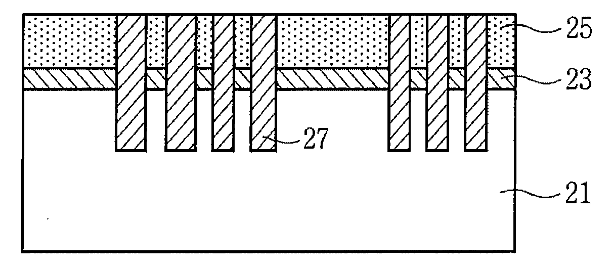
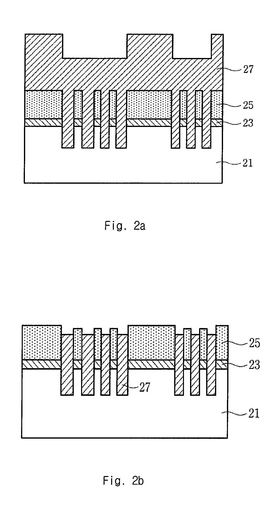
[0015] Since the first polishing process is performed with a slurry having a slow polishing selectivity ratio to an insulating film but a faster polishing selectivity ratio to a tungsten film, the polishing process can be instantly stopped when the insulating film is exposed. However, a dishing and erosions are generated over the tungsten 20 pattern. The second polishing process is subsequently performed with the reverse selective slurry having a high polishing speed to the insulating film so as to remove the dishing and the erosion generated in the first polishing process, thereby planarizing the substrate.

Problems solved by technology

The irregularity affects the next step that makes it difficult to obtain a desired shape.
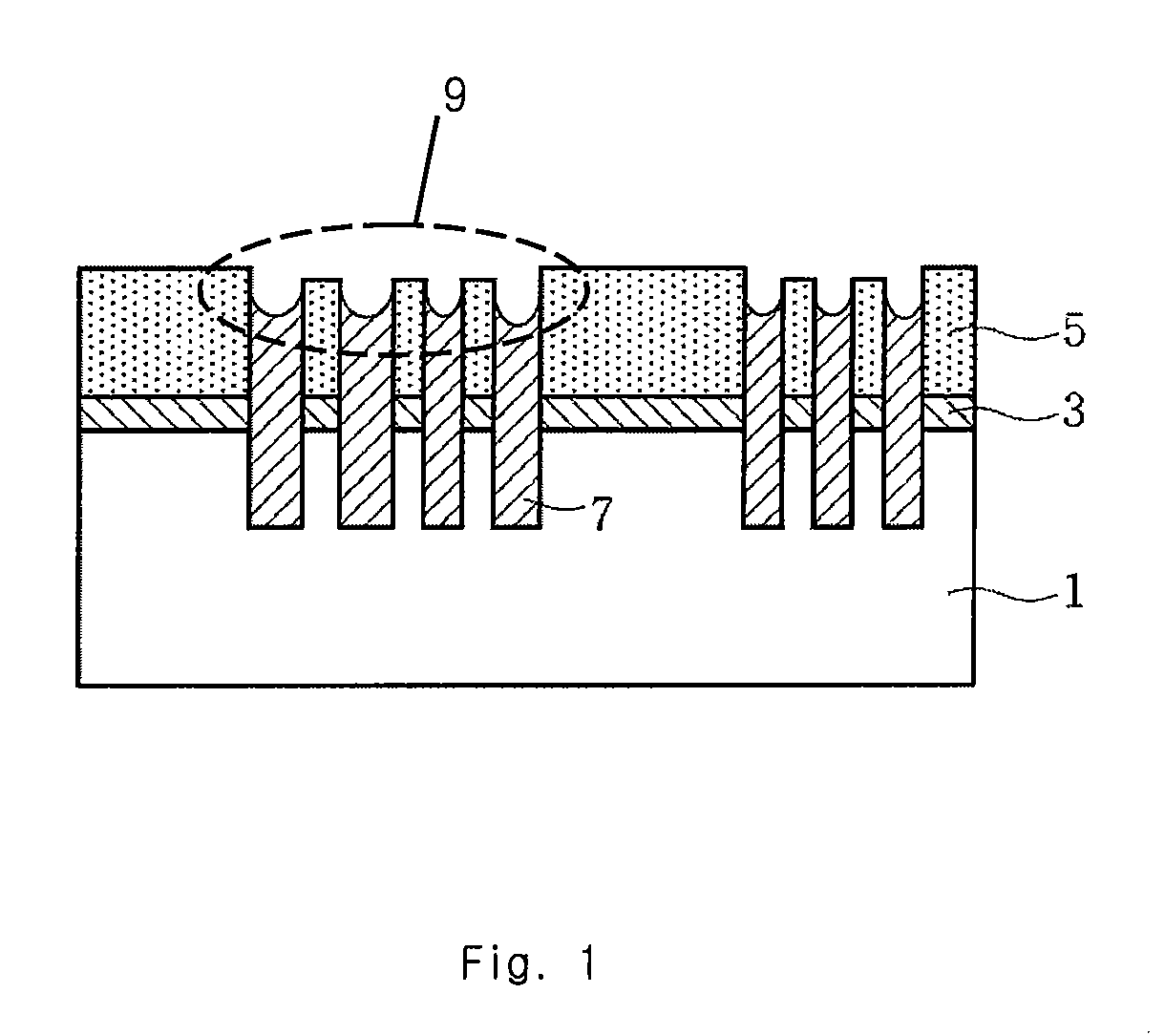
However, the slurry for polishing tungsten causes an erosion in a region where tungsten patterns are densely disposed.

Method used


Image

  • Slurry composition for forming tungsten pattern and method for manufacturing semiconductor device using the same
  • Slurry composition for forming tungsten pattern and method for manufacturing semiconductor device using the same
  • Slurry composition for forming tungsten pattern and method for manufacturing semiconductor device using the same

Examples


example 1

Preparation of a Slurry Composition

[0055] The fumed silica abrasive (the first particle size: 20 nm) was added and stirred into ultra-pure water according to Table 1, and then the pH of the slurry is changed to obtain a slurry of the present embodiment. The fumed silica in the slurry has a secondary average particle size of 140 nm. The planarization wafer (produced by Hynix Semiconductor Inc.) was polished with the slurry, thereby obtaining a polishing selectivity ratio of the insulating film (PETEOS) to tungsten as shown in Table 1. The polishing selectivity ratio was estimated using an Unipla 211 produced by DOOSAN DND Co.

TABLE 1silicapolishingcontenttungsten (W)selectivity(parts byPETEOS polishingpolishing speedratioweight)pHspeed (Å / min)(Å / min)(PETEOS / W)5.721151585.71074712625.710.98751367

The silica content is based on 100 parts by weight of the slurry.

[0056] Referring to Table 1, the selectivity (PETEOS / W) shows more than 3, and the fumed silica has the higher polishing se...

example 2

Preparation of a Slurry Composition and a Polishing Selectivity Ratio Thereof

[0058] The colloidal silica abrasive and methanol (0.05 parts by weight, based on 100 parts by weight of the slurry) as an alcohol organic compound were added and stirred into ultra-pure water according to the rate of Table 2, and then the pH of the slurry is changed to obtain a slurry of the present embodiment. The planarization wafer (produced by Hynix Semiconductor Inc.) was polished with the slurry, thereby obtaining a polishing selectivity ratio of insulating film (PETEOS) to tungsten as shown in Table 2. The polishing selectivity ratio was estimated using a Poli500 CE produced by G&P Technology Co.

TABLE 2silicaPETEOStungsten (W)polishingparticlecontentpolishingpolishingselectivitysize(parts byspeedspeedratio(nm)weight)pH(Å / min)(Å / min)(PETEOS / W)45102.3126445281010.51535305080102.3161160271010.529204467

The silica content is based on 100 parts by weight of the slurry.

[0059] Table 2 shows that the sl...

example 3

Preparation of a Slurry Composition and a Polishing Selectivity Ratio Thereof

[0060] The fumed silica abrasive (the first particle size: 20 nm) and glycine (0.04 parts by weight, based on 100 parts by weight of the slurry) as a complexing agent were added and stirred into ultra-pure water according to the rate of Table 3, and then the pH of the slurry is changed to obtain a slurry of the present embodiment. The fumed silica in the slurry has a secondary average particle size of 140 nm. The planarization wafer (produced by Hynix Semiconductor Inc.) was polished with the slurry, thereby obtaining a polishing selectivity ratio of the insulating film (PETEOS) to tungsten as shown in Table 3. The polishing selectivity ratio was estimated using an Unipla 211 produced by DOOSAN DND Co.

TABLE 3silicatungstencontentComplexingPETEOS(W)polishing(partsagentpolishingpolishingselectivityby(parts byspeedspeedratioweight)weight)pH(Å / min)(Å / min)(PETEOS / W)5.70.0410.987119465.711.98751367

The silica ...


PUM


Abstract

A method for manufacturing a semiconductor device with a slurry composition for forming a tungsten pattern. The method comprises: forming a trench in an insulating film formed on a substrate; depositing a tungsten film over the insulating film including the trench; first polishing a tungsten film with a first slurry for polishing metal to expose the insulating film, the polishing selectivity ratio of the first slurry onto tungsten / insulating film being range from 30 to 100; and second polishing the insulating film and the tungsten film with a second slurry, the polishing selectivity ratio of the second slurry onto insulating film / tungsten being range from 3 to 500. The method reduces a thickness difference of tungsten patterns, thereby improving a production yield of semiconductor devices.

Description

CROSS-REFERENCES TO RELATED APPLICATIONS [0001] The present application claims priority to Korean patent application number 10-2006-0094347 and 10-2007-0096133, respectively filed on Sep. 27, 2006 and Sep. 20, 2007, which are incorporated by references in their entireties. BACKGROUND OF THE INVENTION [0002] The present invention relates to a slurry composition used in forming a tungsten pattern, and a method for manufacturing a semiconductor device using the same. [0003] As a semiconductor device becomes smaller and the number of metal lines becomes larger, the irregularity of each layer is transferred to the next layer, so that the highest layer from the point of the substrate has the most irregularity. The irregularity affects the next step that makes it difficult to obtain a desired shape. [0004] In order to improve the yield of semiconductor devices, it is necessary to perform a planarization process on the irregular surface to minimize line resistance deviation in a semiconduct...

Claims


Application Information

Patent Timeline
IPC IPC(8): H01L21/4763C09K13/00C09K13/02
CPCC09G1/02C09K3/1409H01L21/3212H01L21/31053C09K3/1463
Inventor KIM, SEOK JUPARK, HYU BUMYANG, KI HONGJIN, GYU AN
Owner SK HYNIX INC
Learn More