Phase Change Memory, Phase Change Memory Assembly, Phase Change Memory Cell, 2D Phase Change Memory Cell Array, 3D Phase Change Memory Cell Array and Electronic Component

a phase change memory and memory cell technology, applied in the direction of digital storage, semiconductor devices, instruments, etc., can solve the problems of increasing complexity of the structure insufficient current supply to switch a conventional phase change memory, etc., and achieve the effect of keeping the structure design of the phase change memory simpl

Active Publication Date: 2008-05-01
RWTH AACHEN UNIVERSITY +1
View PDF18 Cites 112 Cited by
  • Summary
  • Abstract
  • Description
  • Claims
  • Application Information

AI Technical Summary

Benefits of technology

[0011] The object of the present invention is to provide a phase change memory and components built thereon, wherein the switching current of a current signal and the heat loss vi

Problems solved by technology

To this end, it must be possible for a phase change memory to be switched by means of the smallest possible switching currents of a current signal, since a phase change memory could otherwise not be operated by future highly integrated CMOS control transistors.
One problem is that the phase change between a crystalline phase and an amorphous phase in the phase change material is induced thermally via a current pulse of the current signal, e.g. using a temperature range between room temperature and 600° C. The current signal is fed into the phase change memory via the electrical contacts, which are usually made of metal, such that a switching zone of a memory material layer is traversed by the current signal.
Since electrical conductors are usually also good heat conductors, this means in the conventional concepts of a phase change memory

Method used


Image

  • Phase Change Memory, Phase Change Memory Assembly, Phase Change Memory Cell, 2D Phase Change Memory Cell Array, 3D Phase Change Memory Cell Array and Electronic Component
  • Phase Change Memory, Phase Change Memory Assembly, Phase Change Memory Cell, 2D Phase Change Memory Cell Array, 3D Phase Change Memory Cell Array and Electronic Component
  • Phase Change Memory, Phase Change Memory Assembly, Phase Change Memory Cell, 2D Phase Change Memory Cell Array, 3D Phase Change Memory Cell Array and Electronic Component

Examples


Embodiment Construction

[0063] Embodiments of the invention will be described with reference to the accompanying drawing figures wherein like numbers represent like elements throughout.

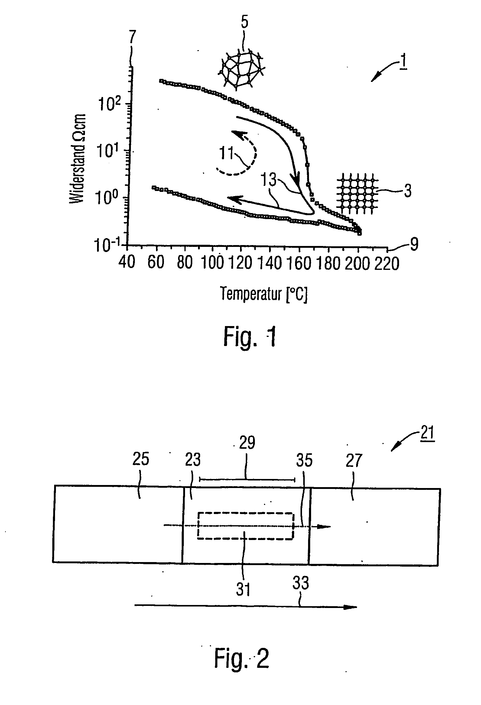
[0064]FIG. 1 shows a resistance / temperature graph 1 recorded at a heating rate of 23° C. per minute, which illustrates in principle the phase change between a crystalline phase 3 and an amorphous phase 5 and thus a change in resistance 7 of a phase change material in a switching zone of a memory material layer of a phase change memory. The change in resistance 7 is thermally induced in a phase change memory by means of a current signal via a change in temperature 9. A preferred chalcogenide phase change material may be both in a stable crystalline phase 3 and in a meta-stable amorphous phase 5 at room temperature. The reversible phase transformation within the context of an amorphization or crystallization between the two phases 5, 3 is accompanied by a significant change in electrical resistance 7 and thus is used to store...


PUM


Abstract

A phase change memory having a memory material layer consisting of a phase change material, and a first and second electrical contact which are located at a distance from one another and via which a switching zone of the memory material layer can be traversed by a current signal, wherein the current signal can be used to induce a reversible phase change between a crystalline phase and an amorphous phase and thus a change in resistance of the phase change material in the switching zone. The invention also relates to a phase change memory assembly, a phase change memory cell, a 2D phase change memory cell array, a 3D phase change memory cell array and an electronic component.

Description

CROSS REFERENCE TO RELATED APPLICATIONS [0001] This is the U.S. national phase of International Application No. PCT / EP04 / 11812, filed Oct. 19, 2004 which claims priority to German Application No. 103 49 750.1, filed Oct. 23, 2003.BACKGROUND OF THE INVENTION [0002] The invention relates to a phase change memory comprising a memory material layer consisting of a phase change material, and a first and second electrical contact which are located at a distance from one another and via which a switching zone of the memory material layer can be traversed by a current signal, wherein the current signal can be used to induce a reversible phase change between a crystalline phase and an amorphous phase and thus a change in resistance of the phase change material in the switching zone. The invention also relates to a phase change memory assembly, a phase change memory cell, a 2D phase change memory cell array, a 3D phase change memory cell array and an electronic component. [0003] One of the es...

Claims


Application Information

Patent Timeline
IPC IPC(8): G11C11/00H01L27/24H01L45/00
CPCH01L27/2409H01L27/2436H01L27/2481H01L45/1675H01L45/1226H01L45/1246H01L45/144H01L45/06H10B63/84H10B63/20H10B63/30H10N70/828H10N70/823H10N70/231H10N70/8828H10N70/063
Inventor HARING-BOLIVAR, PETERBECHEVET, BERNARDSOUSA, VERONIQUEKIM, DAE-HWANGKURZ, HEINRICHMERGET, FLORIAN
Owner RWTH AACHEN UNIVERSITY
Why Eureka
Try Eureka