
Test system of digital video data and semiconductor device

a technology of semiconductor devices and test systems, applied in the direction of signal generators with optical-mechanical scanning, color televisions with bandwidth reduction, signal systems, etc., to achieve the effect of minimizing the increase of circuit area

Inactive Publication Date: 2008-05-01
PANASONIC CORP
View PDF10 Cites 18 Cited by
  • Summary
  • Abstract
  • Description
  • Claims
  • Application Information

AI Technical Summary

Benefits of technology

[0023]A yet another object of the present invention is minimizing increase in circuit area resulting from mounting of an exclusive circuit for testing in a semiconductor device to be tested.
[0027]The timing of code generation for each digital video data unit may be shifted, to permit sharing of a memory element for temporary data holding among digital video data units. This greatly reduces the area of the memory element.

Problems solved by technology

The conventional digital video data test systems described above however have the following problems.

Method used


Image

  • Test system of digital video data and semiconductor device
  • Test system of digital video data and semiconductor device
  • Test system of digital video data and semiconductor device

Examples


embodiment 1

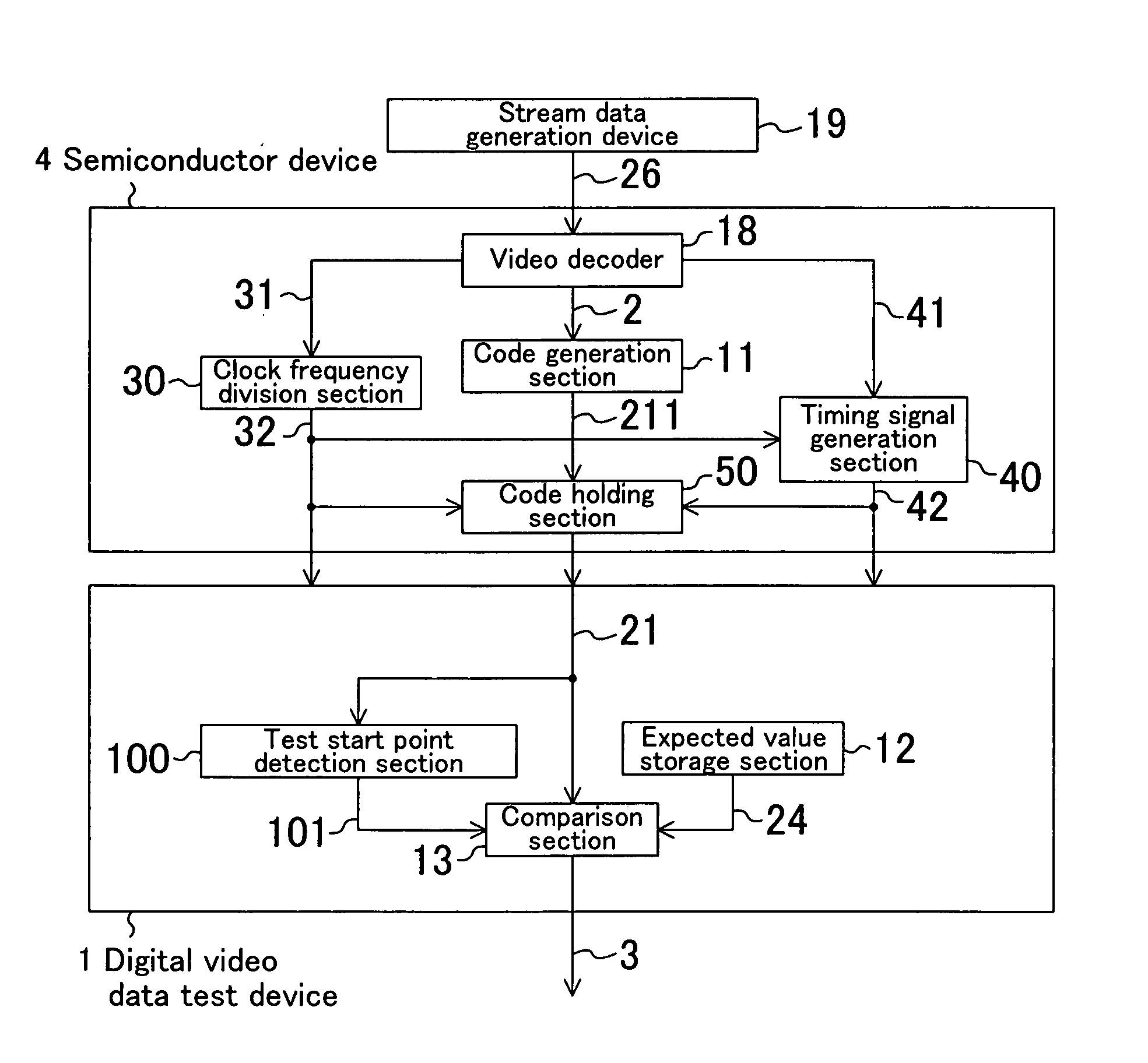
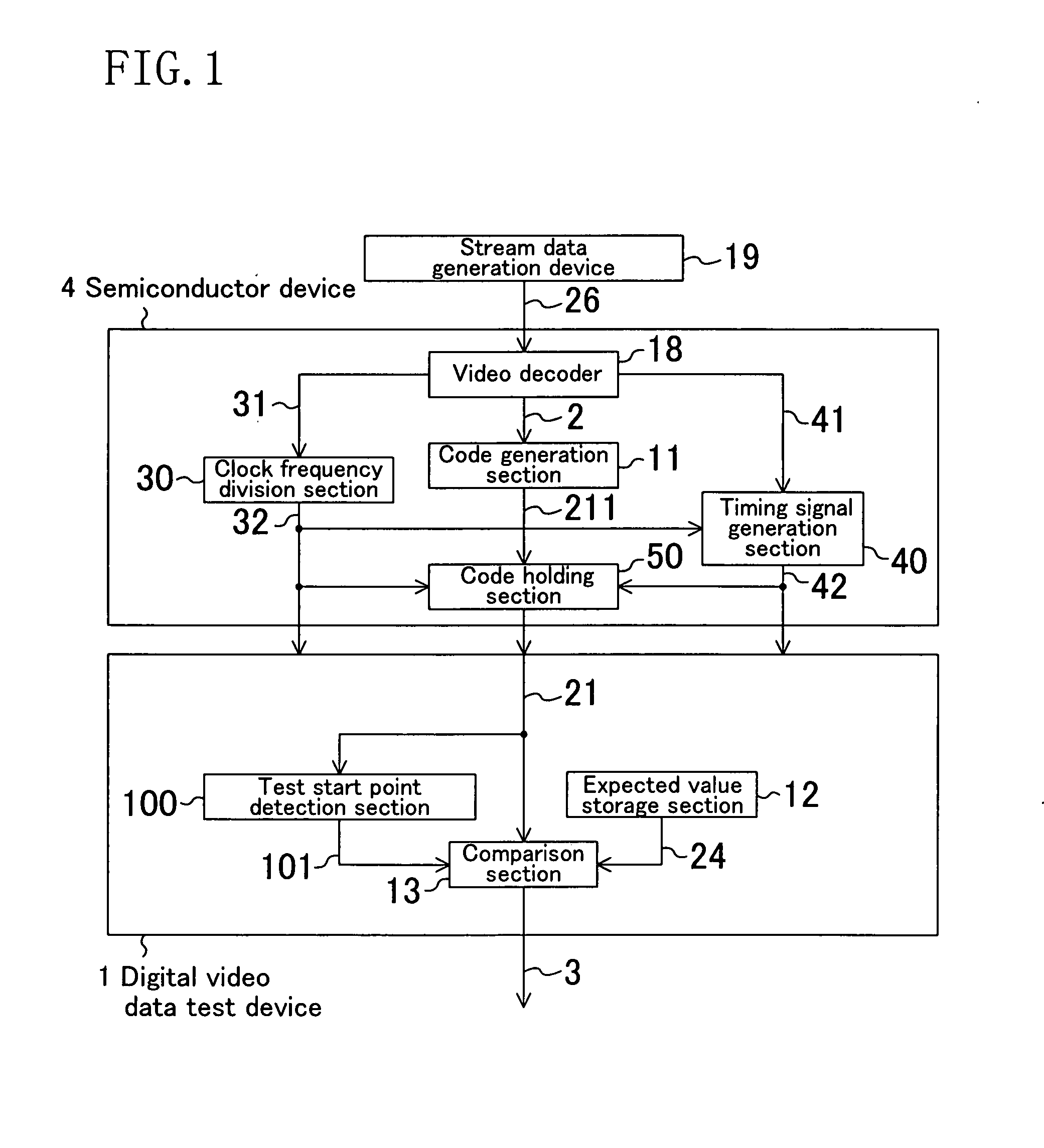
[0075]FIG. 1 is a block diagram showing the entire configuration of a digital video data test system of Embodiment 1 of the present invention.

[0076]In FIG. 1, a stream data generation device 19 outputs stream data 26. A semiconductor device 4, which is an object to be tested, processes the stream data 26 and outputs a generated code 21. A digital video data test device 1 processes the generated code 21 to test the semiconductor device 4. The semiconductor device 4 and the digital video data test device 1 constitute the digital video data test system.

[0077]The semiconductor device 4 includes: a video decoder 18 for processing the stream data 26 to generate digital video data 2; a code generation section 11 for generating a code (generated code) 211 uniquely defined from the digital video data 2; a clock frequency division section 30 for dividing the frequency of a digital video clock 31 to generate a frequency-divided clock 32; a timing signal generation section 40 for generating a t...

embodiment 2

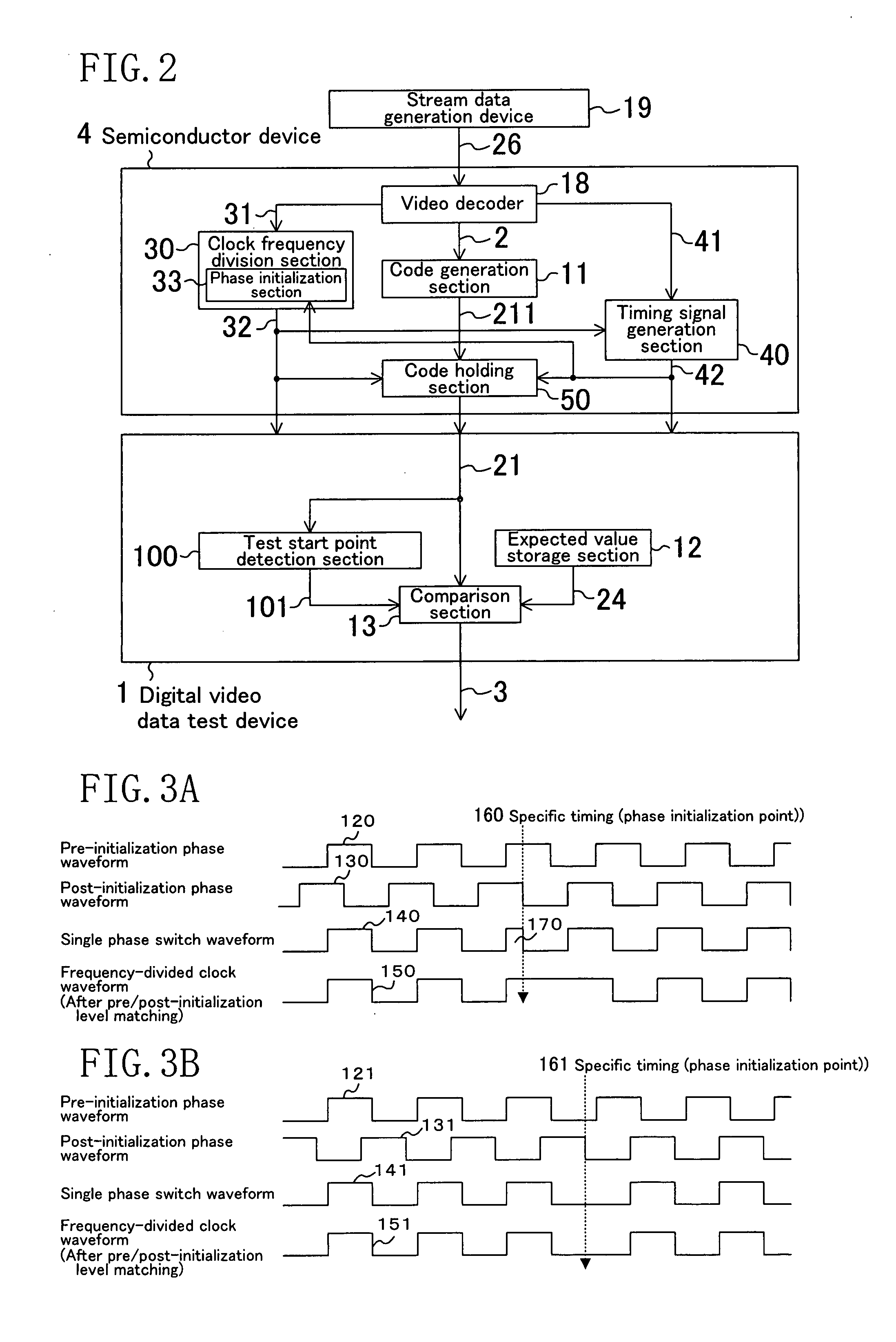
[0089]FIG. 2 is a block diagram showing the entire configuration of a digital video data test system of Embodiment 2 of the present invention.

[0090]The digital video data test system of this embodiment is different from that of Embodiment 1 described above in that a phase initialization section 33 is additionally provided. If the test timing interval is not an integral multiple of the frequency-divided clock, the phase of the frequency-divided clock must be initialized. In this case, the signal level may differ between before and after the initialization, and this may cause generation of a pulse having a length shorter than the half cycle of the frequency-divided clock. The phase initialization section 33 is provided to avoid such an occurrence. The other part of the configuration is the same as that of Embodiment 1. The same components are therefore denoted by the same reference numerals and only the point different from Embodiment 1 will be described.

[0091]In the semiconductor dev...

embodiment 3

[0099]FIG. 4 is a block diagram showing the entire configuration of a digital video data test system of Embodiment 3 of the present invention.

[0100]The digital video data test system of this embodiment is different from that of Embodiment 1 described above in that a code generation initialization section 46 is additionally provided. The code generation initialization section 46 initializes the code generation section 11 with an initialization value reflecting the digital video data 2 in the initialization cycle, in synchronization with the timing signal 42. The other part of the configuration is the same as that of Embodiment 1. The same components are therefore denoted by the same reference numerals and only the point different from Embodiment 1 will be described.

[0101]In the semiconductor device 4, the code generation section 11 receives the timing signal 42 and is provided with the code generation initialization section 46 that initializes the code generation section 11 with an i...


PUM


Abstract

The digital video data test system includes a semiconductor device to be tested and a digital video data test device. In the semiconductor device, a clock frequency division section divides the frequency of a digital video clock to generate a frequency-divided clock. A timing signal generation section generates a timing signal synchronizing with the frequency-divided clock using a sync signal in digital video data. A code holding section outputs a generated code generated by a code generation section to the digital video data test device in synchronization with the timing signal and the frequency-divided clock.

Description

CROSS-REFERENCE TO RELATED APPLICATIONS[0001]This application claims priority under 35 U.S.C. §119 on Patent Application No. 2006-298061 filed in Japan on Nov. 1, 2006, the entire contents of which are hereby incorporated by reference.BACKGROUND OF THE INVENTION[0002]The present invention relates to a semiconductor device handling digital video data and a digital video data test system for detecting an electrical failure of the semiconductor device.[0003]Japanese Laid-Open Patent Publication No. 2006-128905 discloses a digital video data test system and test device, in which a code uniquely defined from digital video data is generated inside a semiconductor device to be tested, and the generated code is compared with an expected value code inside or outside the semiconductor device, to thereby test the semiconductor device.[0004]FIG. 16 is a block diagram showing the entire configuration of a conventional digital video data test system.[0005]In FIG. 16, a stream data generation devi...

Claims


Application Information

Patent Timeline
Patent Type & Authority Applications(United States)
IPC IPC(8): H04B1/66
CPCH04N17/045H04N17/004
Inventor ISHIKAWA, KAZUNOBU
Owner PANASONIC CORP
Learn More