Plasma processing device and plasma processing method

a processing device and plasma technology, applied in the field of plasma processing devices, can solve the problems damaging the dielectric window, and the processing chamber becoming smaller, and achieve the effect of increasing the thermal stress created by plasma

Inactive Publication Date: 2008-05-08
SHARP KK
View PDF5 Cites 26 Cited by
  • Summary
  • Abstract
  • Description
  • Claims
  • Application Information

AI Technical Summary

Benefits of technology

[0013] As described above, a conventional plasma processing device for performing desired plasma processing by generating large-area, uniform and high-density plasma using microwave discharge of non-magnetic field entails the following drawback. That is, if the area of substrate to be processed is increased or a high-speed process is achieved, the risk of damaging the dielectric window due to the dynamic stress caused by the difference in the pressured applied to the dielectric window used for inputting microwave, and thermal stress created by plasma is increased.
[0015] On the other hand, the technique disclosed in Jpn. Pat. Appln. KOKAI Publication No. 11-026187 has the following features. That is, first, another vacuum pump which is separate from the main vacuum pump provided for the processing chamber is installed in the waveguide and thus the waveguide is evacuated by this vacuum pump, and secondly, the pressure is set to such that abnormal discharge does not occur inside the wave guide (1.33×10³ Pa or more at 1 kW). However, the separately provided vacuum pump is provided on the microwave input side, and thus this technique is applicable only in the special transmission and radiation method of microwave (or a device that utilizes a dielectric waveguide path). In other words, this technique is not applicable to the most popular method, which is the microwave discharge method that uses a slot antenna directly connected to a waveguide. Further, in connection with the second aspect described above, the pressure to prevent abnormal discharge is increased as the power of microwave is increased. Therefore, the pressure, at 10 kW, is 13.3×10³ Pa or more, which is close to the atmospheric pressure. It becomes impossible to decrease the thickness of the dielectric plate.
[0018] Therefore, an object of the present invention is to provide a plasma processing device which can generate uniform and high-density large-area plasma while preventing abnormal discharge and reduce the dynamic stress and thermal stress applied to a dielectric window for microwave input, generated by the plasma, as well as a processing method using plasma.

Problems solved by technology

That is, if the area of substrate to be processed is increased or a high-speed process is achieved, the risk of damaging the dielectric window due to the dynamic stress caused by the difference in the pressured applied to the dielectric window used for inputting microwave, and thermal stress created by plasma is increased.
That is, since it is necessary to provide a sealing material for sealing vacuum for the number of coupling holes in this reference technique, the structure of the processing chamber becomes complicated, and the number of parts is increased, thereby making the cost of the device high.
As a result, plasma becomes ununiform in some cases especially when the atmosphere in the chamber is at a high pressure.
In other words, this technique is not applicable to the most popular method, which is the microwave discharge method that uses a slot antenna directly connected to a waveguide.

Method used


Image

  • Plasma processing device and plasma processing method
  • Plasma processing device and plasma processing method
  • Plasma processing device and plasma processing method

Examples


first embodiment

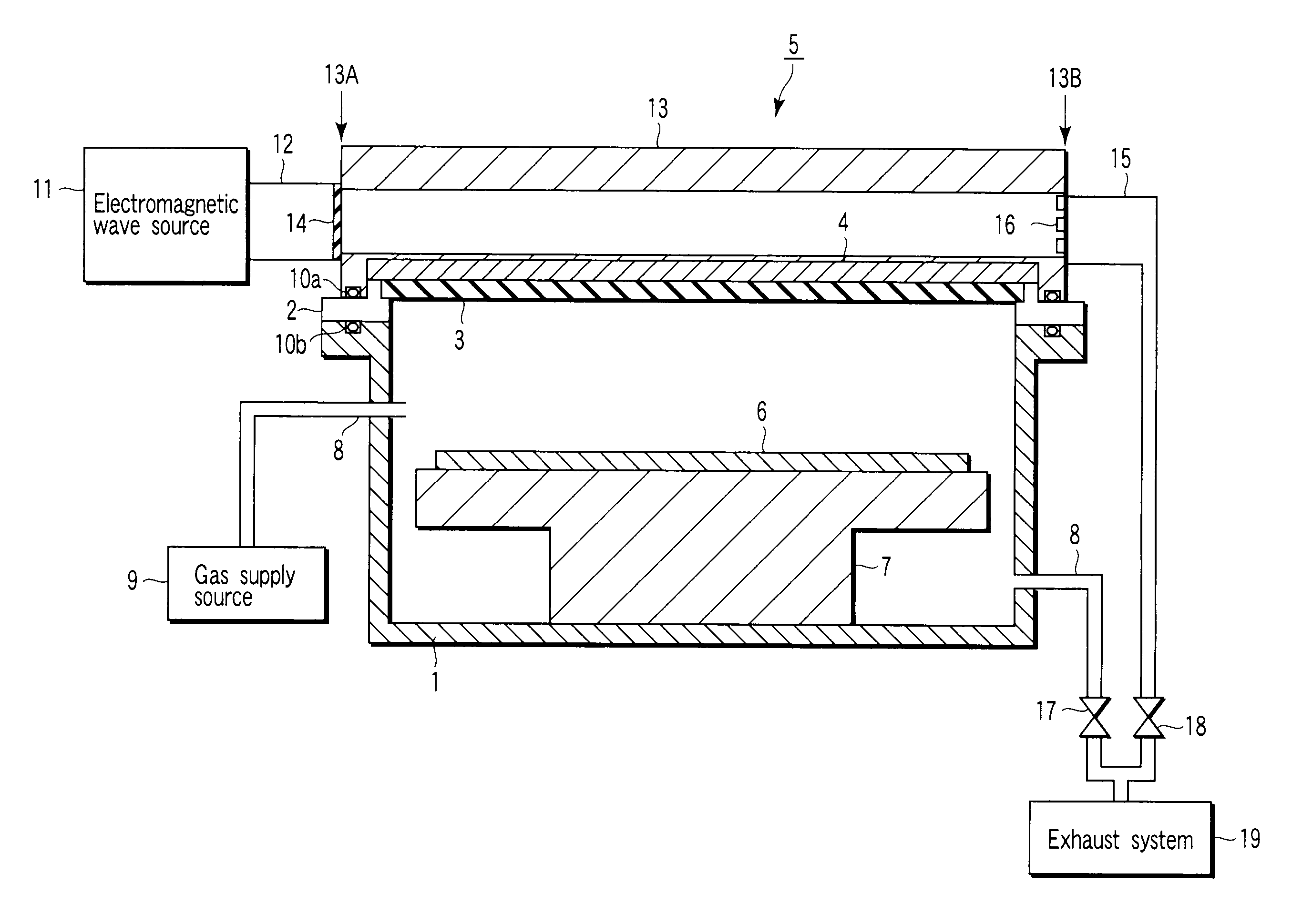
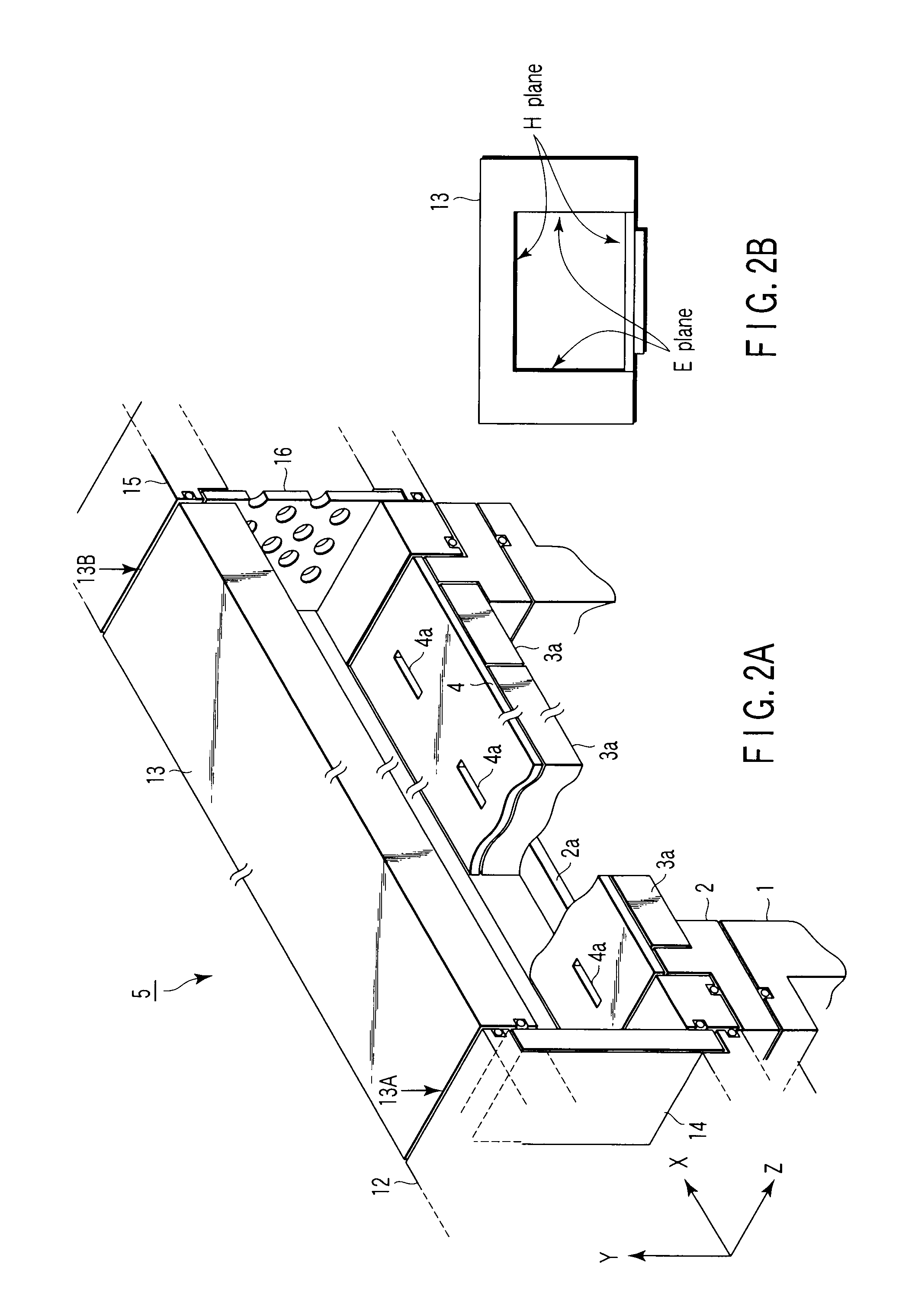
[0031]FIG. 1 illustrates a conceptual cross sectional structure of a plasma-using processing device taken in the longitudinal direction (microwave traveling direction) of the vacuum waveguide. FIG. 2A is diagram showing the structure of the plasma processing device of FIG. 1 when viewed from above in an oblique direction, and FIG. 2B is diagram showing a E plane and H plane of the vacuum waveguide.

[0032] This plasma processing device includes a processing chamber 1 in which a substrate stage 7 on which a substrate 6 to be processed, which can be mainly divided into a silicon substrate, or a glass substrate or the like, and a processing gas supply tube are provided, a ring-shaped spacer 2 provided air-tightly on an upper end portion of the processing chamber 1, a first dielectric member 3 fit into a notch made in an inner side of the spacer 2, and a microwave radiation system provided on the spacer 2 and radiating electromagnetic wave, for example, microwave to the processing chambe...

second embodiment

[0073] Next, a plasma-using processing device according to the present invention will now be described with reference to FIG. 5, which illustrates the conceptual structure of the device.

[0074] With regard to the structural parts of this embodiment, similar parts to those already discussed in the first embodiment will be designated by the same reference symbols, and the detailed explanations therefore will not be repeated.

[0075] The above-described first embodiment was explained in connection with an example in which a microwave radiating system including one electromagnetic wave source 11 and one vacuum waveguide 13 is mounted in the plasma processing device. In an actual occasion where a vacuum waveguide 13 which uses microwave is mounted in a plasma processing device, such a microwave radiating system including one electromagnetic wave source 11 and one vacuum waveguide 13 may be practical if the substrate to be processed has a relatively small area having a diameter of a silicon...


PUM

PropertyMeasurementUnit
pressureaaaaaaaaaa
pressureaaaaaaaaaa
pressureaaaaaaaaaa

Abstract

A plasma processing device reduces the pressure inside a vacuum waveguide which propagates microwave to a vacuum of a high degree, thereby preventing abnormal discharge in the vacuum waveguide and around a slot plate, and reduces the difference in pressure between the processing chamber and the vacuum waveguide, thereby lowering the stress applied on the slot plate and a dielectric member for generating surface plasma, thus carrying out high-quality plasma processing.

Description

CROSS REFERENCE TO RELATED APPLICATIONS [0001] This is a Continuation Application of PCT Application No. PCT / JP2006 / 313123, filed Jun. 30, 2006, which was published under PCT Article 21(2) in Japanese. [0002] This application is based upon and claims the benefit of priority from prior Japanese Patent Application No. 2005-196555, filed Jul. 5, 2005, the entire contents of which are incorporated herein by reference.BACKGROUND OF THE INVENTION [0003] 1. Field of the Invention [0004] The present invention relates to a plasma processing device equipped with a waveguide which propagates electromagnetic waves (microwaves), and a processing method which uses plasma. [0005] 2. Description of the Related Art [0006] In general, the process for manufacturing semiconductor devices, liquid crystal display apparatus, etc., includes plasma processing in a step of depositing an oxide film or a conductor film, a surface reforming step such as annealing process, or an etching step of forming a pattern...

Claims


Application Information

Patent Timeline
Patent Type & Authority Applications(United States)
IPC IPC(8): B44C1/22C23F1/00H05H1/24C23C16/00
CPCH01J37/32192H05H1/46H01J37/32834
Inventor SUGAI, HIDEOIDE, TETSUYASASAKI, ATSUSHIAZUMA, KAZUFUMI
Owner SHARP KK
Why Eureka
Try Eureka