

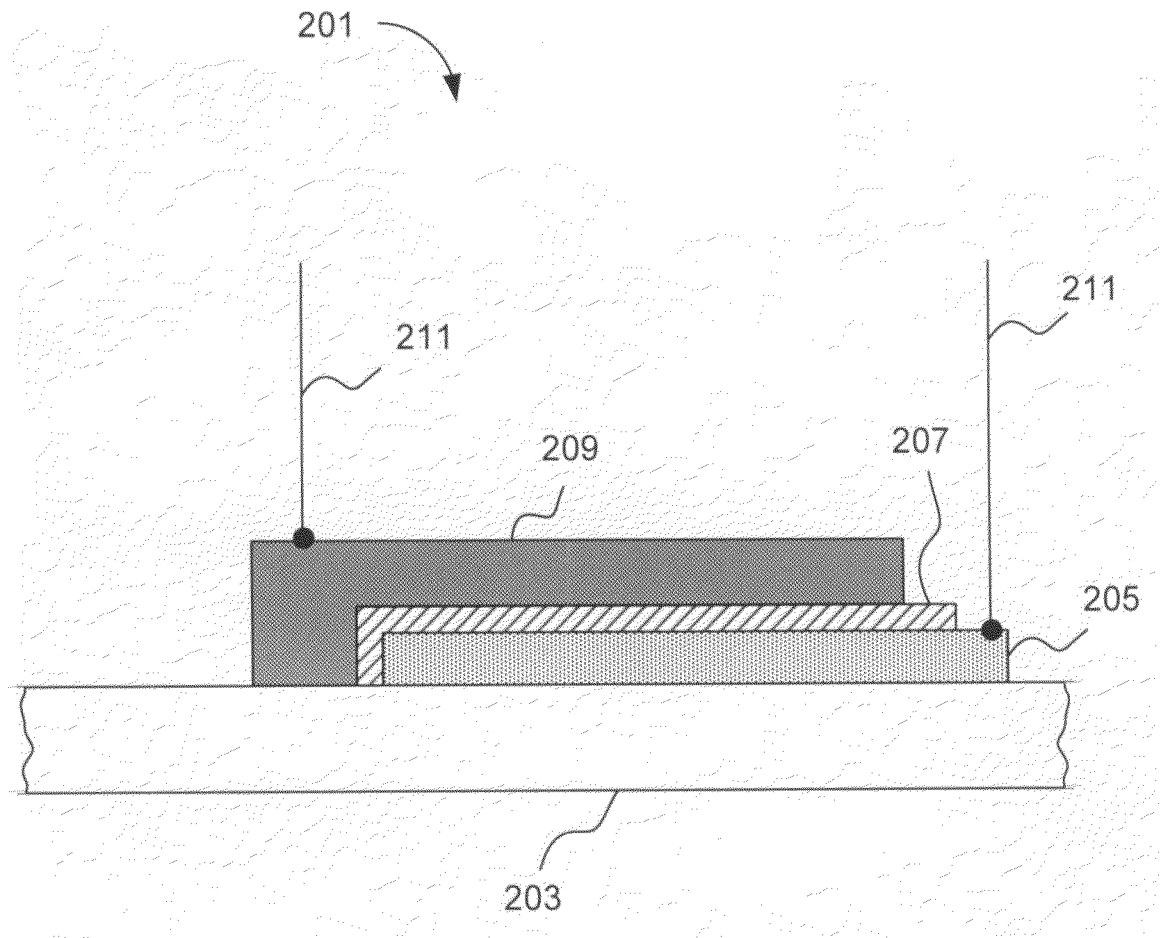
Two-terminal switching devices and their methods of fabrication
a switching device and two-terminal technology, applied in bulk negative resistance effect devices, optics, instruments, etc., can solve the problems of tfd fabrication process typically requiring less precision patterning, tfd fabrication consumes fewer resources than tft fabrication, and tfd fabrication consumes fewer resources. , to achieve the effect of high work function or fermi energy, good device performance, and high forward curren
- Summary
- Abstract
- Description
- Claims
- Application Information
AI Technical Summary
Benefits of technology
Problems solved by technology
Method used
Image

Examples
examples
[0109]Several examples of device compositions are herein illustrated in a cathode / semiconductor layer / anode format:
Ta / Ta2O5-δ / PEDOT:PSS;
Mg / Ta2O5-δ / PEDOT:Ag;
Ta / Ta2O5-δ / MEH-PPV / PEDOT:PSS;
Mg / Ta2O5-δ / ZnxCuyAlzSw;
ZnO / Ta2O5-δ / PEDOT:PSS.
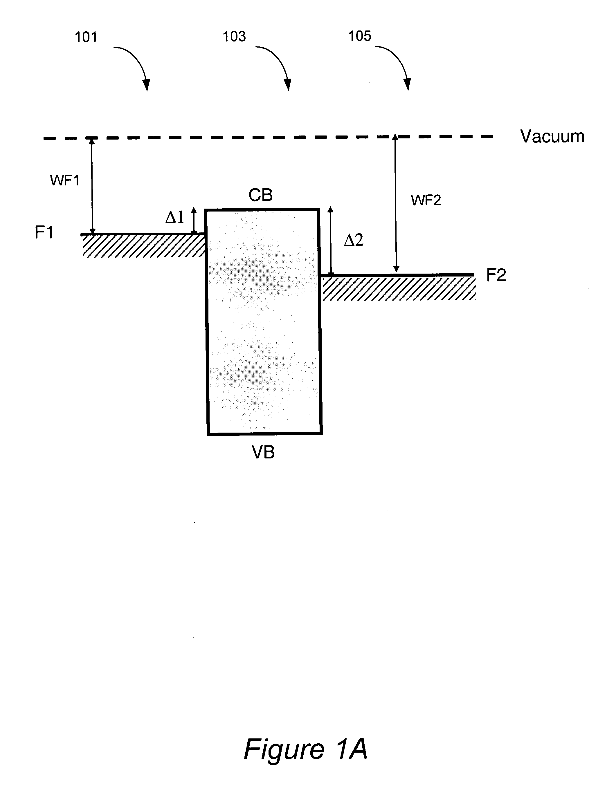
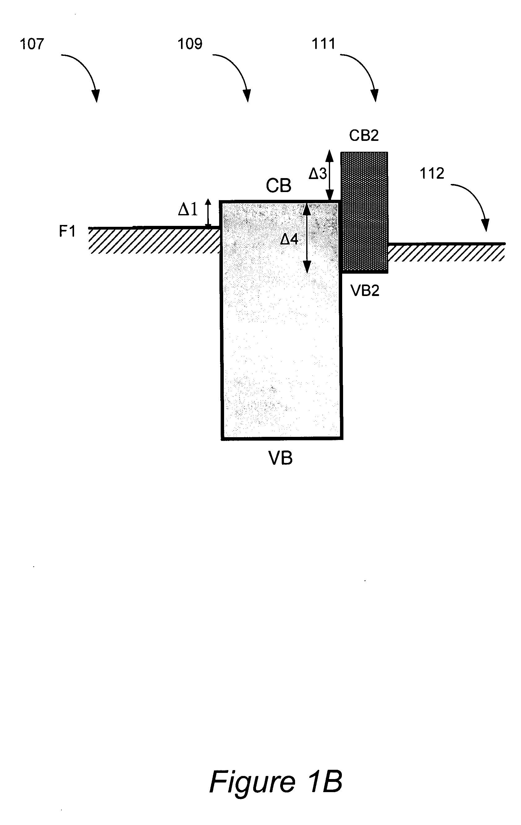
[0110]Other devices can be configured using a variety of material combinations, e.g., using materials presented in Table 1 and Table 2.
TABLE 1Electronic properties of materials suitable for a two-terminal devicewith an organic anode.Semi-AnodeconductorPEDOT:PSSPANI:IPPYPTT:NAFION ®Ca-Ec / Ev;Δ3 (eV)Δ3 (eV)Δ3 (eV)Δ3 (eV)thodeΔ1 (eV)Δ4 (eV)Δ4 (eV)Δ4 (eV)Δ4 (eV)TaTaxOy0.00.40.7−0.53.9 / 7.9; ~0.31.31.10.81.7TiTixOy0.30.71.0−0.14.3 / 7.4; ~0.11.00.80.81.3ZnZnxOy0.30.71.0−0.14.3 / 7.3; ~0.11.00.80.51.3InInxOy0.20.60.9−0.34.1 / 7.6; ~0.11.10.90.61.5ZnZnxSy0.20.60.9−0.34.1 / 7.6; ~0.21.10.90.61.5
[0111]Table 1 illustrates several combinations of materials that can be used in two-terminal switching devices in accordance with electronic guidelines presented herein. Lowest condu...
experimental examples
[0113]A number of two-terminal switching devices have been prepared. Experimental methods used in device fabrication will now be illustrated. Methods used for determining electronic properties of various device materials will also be presented.
example 1
Organic p++ Materials Suitable for Anode Fabrication
[0114]Carrier concentrations were measured for several p++ materials. One example material for which carrier concentrations were determined was PEDOT:PSS, which was purchased from H. C. Starck Chemical (available as BAYTRON P®). The electronic properties of aqueous colloid suspensions of PEDOT having different levels of PSS doping were determined. PEDOT / PSS ratios ranged from between 1:1 to 1:20. Table 3 lists materials used in this study, conductivity of these materials and their carrier densities. It can be seen that conductivity of these materials ranged from about 10−2 S / cm to about 6×10² S / cm.
TABLE 3Electronic parameters of PEDOT:PSSConductivityCarrierIDPEDOT:PSS(S / cm)density (cm−3)1BAYTRON P PH500 ®~300~4 × 10212BAYTRON P PH ® ~0.3~3 × 10183BAYTRON Al 4083 ® ~10−2~1 × 10184BAYTRON P PH ® + 5% DMSO20-501-3 × 10²⁰
[0115]In one example, 100 nm thick PEDOT:PSS (product ID: BAYTRON P PH500®) films were spin-cast onto glass substra...
PUM
| Property | Measurement | Unit |
|---|---|---|
| Temperature | aaaaa | aaaaa |
| Band gap | aaaaa | aaaaa |
| Electric potential / voltage | aaaaa | aaaaa |
Abstract
Description
Claims
Application Information