Split-gate memory cells and fabrication methods thereof

Inactive Publication Date: 2008-05-08
TAIWAN SEMICON MFG CO LTD
View PDF7 Cites 23 Cited by
  • Summary
  • Abstract
  • Description
  • Claims
  • Application Information

AI Technical Summary

Benefits of technology

[0015]The invention further provides a method for fabricating a split-gate memory cell, comprising providing a semiconductor substrate with a plurality of isolation regions along a first direction, between two adjacent isolation regions defining an active region, wherein a top level of the active regions is lower than the top level of the isolation regions. A pair of floating gates is formed on the active regions and aligned with the isolation regions, wherein a passivation layer is conformably

Problems solved by technology

The conventional floating gate, however, is not self-aligned with shallow trench isolation (STI)

Method used


Image

  • Split-gate memory cells and fabrication methods thereof
  • Split-gate memory cells and fabrication methods thereof
  • Split-gate memory cells and fabrication methods thereof

Examples


Embodiment Construction

[0050]The following description is of the best-contemplated mode of carrying out the invention. This description is made for the purpose of illustrating the general principles of the invention and should not be taken in a limiting sense. The scope of the invention is best determined by reference to the appended claims.

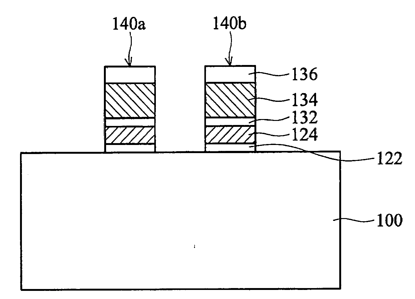
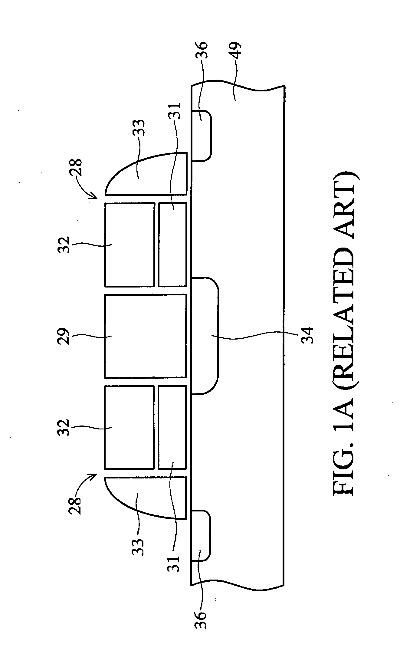
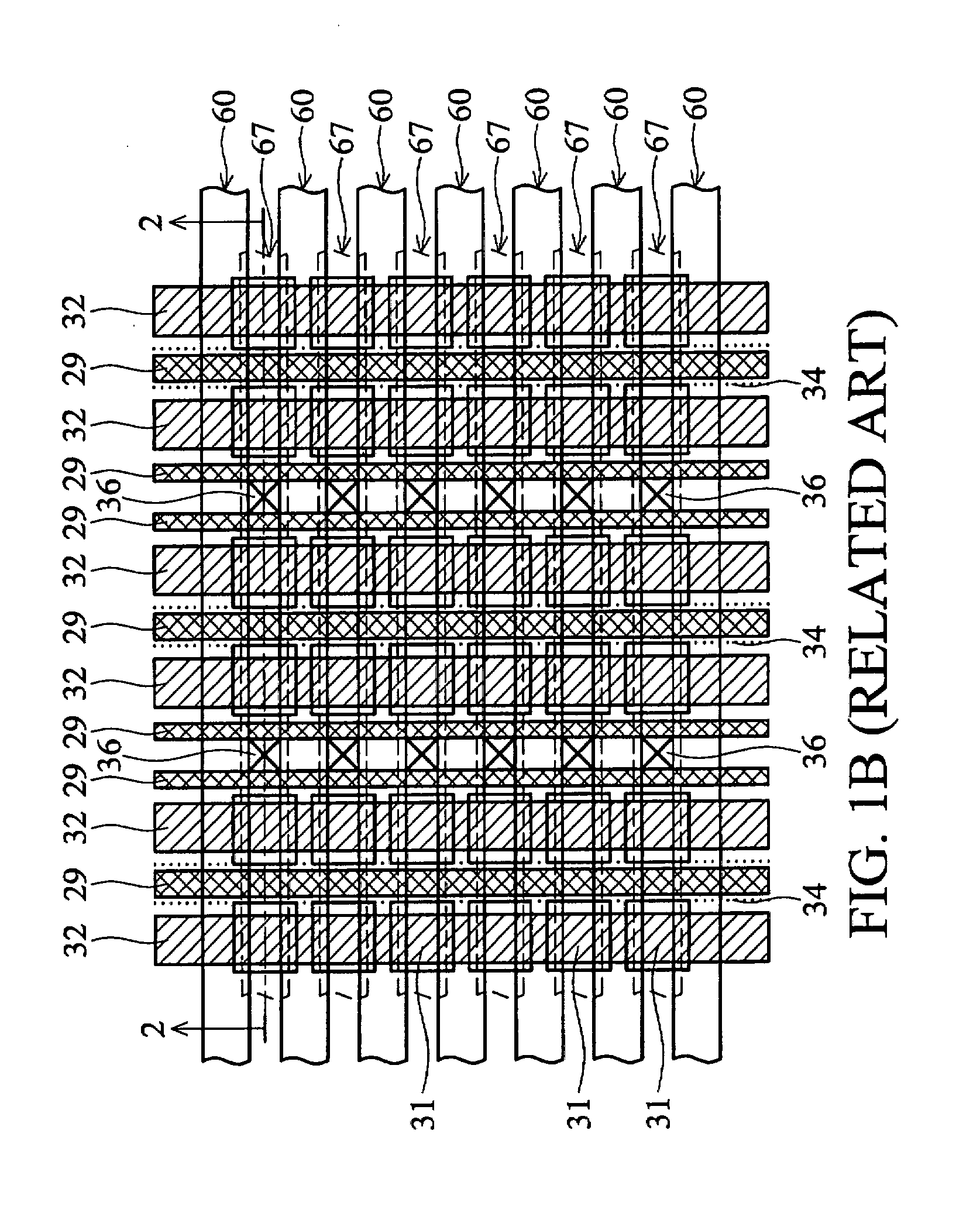
[0051]The invention is directed to split-gate non-volatile memory cells with a floating gate (FG) self-aligned with shallow trench insulators (STI) along a first direction. A control gate (CG) is defined by lithography and self aligned with the floating gate. Moreover, the floating gate is self-aligned with a source line along a second direction. In one aspect of the invention, the source line is formed by a polysilicon source plug directly connected to a source region. In another aspect of the invention, the source line is formed by a self-aligned source (SAS) procedure associated with an SAS-STI etching procedure, and followed by source line implantation. The select ...


PUM


Abstract

Split-gate memory cells and fabrication methods thereof. A split-gate memory cell comprises a plurality of isolation regions formed on a semiconductor substrate along a first direction, between two adjacent isolation regions defining an active region having a pair of drains and a source region. A top level of the active regions is lower than a top level of the isolation regions. A pair of floating gates is disposed on the active regions and aligned with the isolation regions, wherein a passivation layer is disposed on the floating gate to prevent thinning from CMP. A pair of control gates is self-aligned with the floating gates and disposed on the floating gates along a second direction. A source line is disposed between the pair of control gates along the second direction. A pair of select gates is disposed on the outer sidewalls of the pair of control gates along the second direction.

Description

CROSS-REFERENCE TO RELATED APPLICATIONS[0001]The present application is a continuation-in-part of application Ser. No. 11 / 592,290, filed on Nov. 3, 2006, the entirety of which is incorporated herein by reference.BACKGROUND OF THE INVENTION[0002]1. Field of the Invention[0003]The invention relates to electronic memory devices, and more particularly, to self-aligned split-gate memory cells with stacked control gate structures and fabrication methods thereof.[0004]2. Description of the Related Art[0005]Nonvolatile memory, including electrically programmable read only memory (EPROM), electrically erasable programmable read only memory (EEPROM), and flash EEPROM, is currently available in several forms for retaining stored data during periods when no power is applied. Conventionally, non-volatile memory comprises stacked gate and split gate cell structures. The stacked gate memory cells normally have a floating gate and a control gate, with the control gate positioned directly above the ...

Claims


Application Information

Patent Timeline
IPC IPC(8): H01L29/788H01L27/115
CPCH01L27/11521H01L27/115H10B69/00H10B41/30
Inventor HSIEH, CHANG-JENSUNG, HUNG-CHENGCHU, WEN-TINGHUANG, CHEN-MINGKAO, YA-CHENLIU, SHIH-CHANGLO, CHI-HSINYU, CHUNG-YITSAI, CHIA-SHIUNG
Owner TAIWAN SEMICON MFG CO LTD
Why Eureka
Try Eureka