Method for preparing silicon inverse epitaxial wafer and special equipment thereof

A manufacturing method and technology for silicon epitaxial wafers, applied in chemical instruments and methods, from chemical reactive gases, single crystal growth, etc., can solve the problems of low concentration, no large, thick epitaxial layer, etc.

Active Publication Date: 2008-11-26
NANJING GUOSHENG ELECTRONICS
View PDF0 Cites 10 Cited by
  • Summary
  • Abstract
  • Description
  • Claims
  • Application Information

AI Technical Summary

Problems solved by technology

[0009] For the three basic requirements of reverse epitaxial wafers, the thickness of the

Method used


Image

  • Method for preparing silicon inverse epitaxial wafer and special equipment thereof

Examples


Embodiment Construction

[0016] The specific embodiment of the present invention is described in detail below:

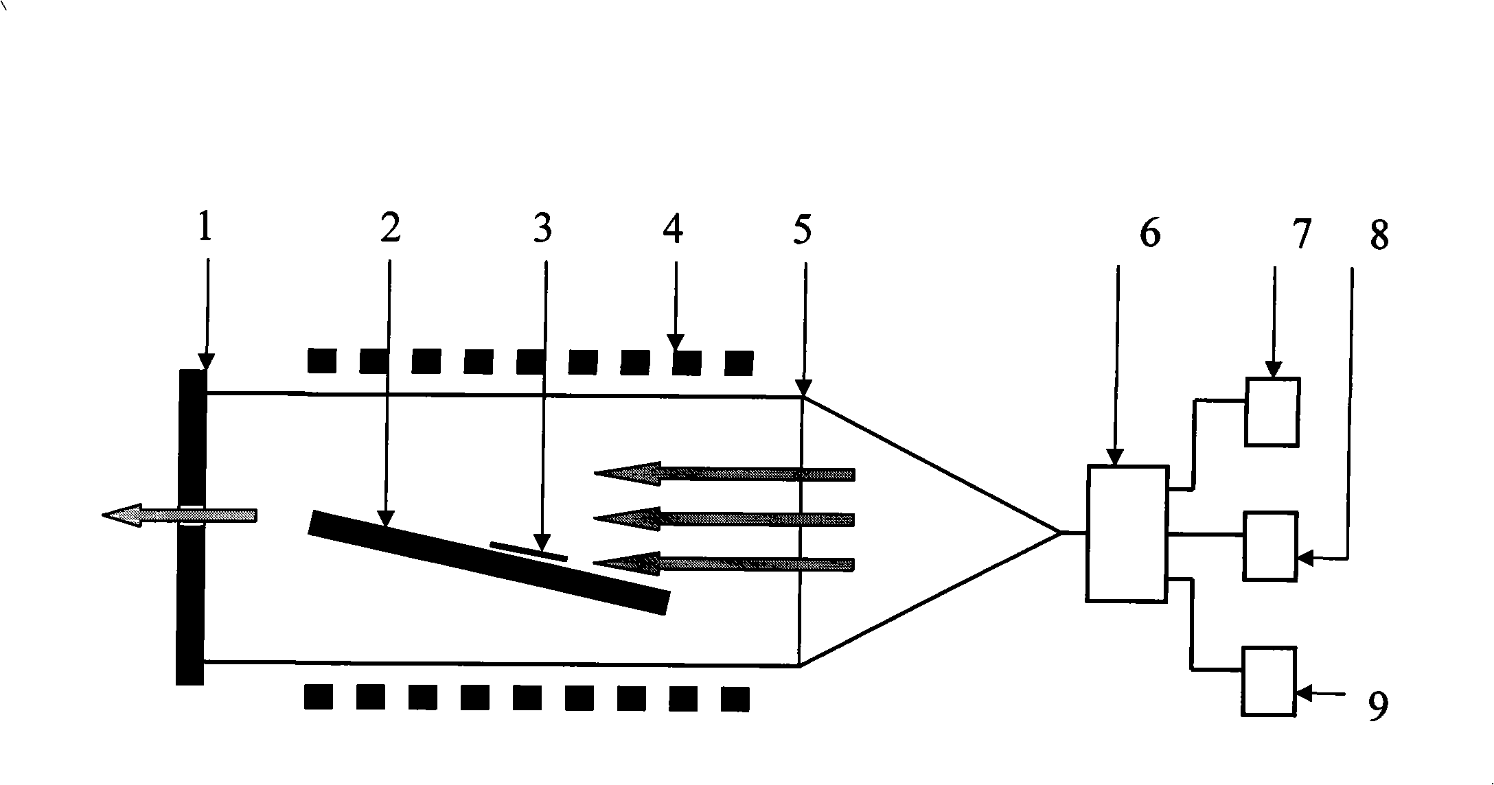
[0017] The used special equipment of the present invention is referring to figure 1 , H 2 Supply source 7, SiHCL 3 and PCl 3 The source 8 and the HCL source 9 are connected to the reactor 5 through the gas control system 6, the reactor 5 is sealed by the reactor sealing cover, the high frequency heating coil 4 is arranged around the reactor 5, and the base 2 is installed in the reactor 5. The reactor 5 is made of a rectangular quartz tube, and the base 2 is made of high-purity graphite after cracking treatment. The size is 80mm×200mm×10mm. The included angle is conducive to high-frequency induction heating, and the temperature of the graphite base can reach 1200 °C. Palladium Tube Furnace for Hydrogen Purifier.

[0018] Reactor and substrate cleaning: The quartz reaction tube and the quartz support must be carefully cleaned before epitaxy to remove impurities and residues adsorbed on t...


PUM


Abstract

The invention discloses a manufacturing method of a silicon inversion epitaxial wafer. First, anti-epitaxial equipment specially used for the silicon inversion epitaxial wafer is designed and manufactured; the liquidoid doping technology of epitaxial layer is adopted; the epitaxial process conditions which are suitable for the silicon inversion epitaxial wafer is built. The liquidoid doping technology of the epitaxial layer is that PC13 is added into SiHCL3 and the mixture ratio is suitable for satisfying the resistivity of the epitaxial layer; one kilogram of SiHCL3 is added with 5ml of PC13. The suitable process conditions are that gaseous temperature is 1190 DEG C, gaseous flow is 20 liters per minute, growing temperature is 1180 DEG C and the growing speed is 5Mum per minute. The flatness of the surface of the epitaxial wafer and the lattice integrity of the epitaxial wafer are ensured while the doping concentration of the epitaxial wafer is ensured.

Description

1. Technical field [0001] The invention relates to a method for manufacturing a silicon reverse epitaxial wafer, in particular to a method for manufacturing a silicon reverse epitaxial wafer for a high-voltage PIN switch tube and special equipment thereof. 2. Background technology [0002] Silicon epitaxy is a technique in which the grown atoms are ordered in a single crystal on the surface of the substrate and the crystal structure of the growth layer is exactly the same as that of the substrate. The most important reason for applying this technique is the ease and control of impurities in the epitaxial layer. The epitaxial material used in the high-voltage PIN switch requires that the resistivity of the flat area is greater than 1000Ωcm, the width of the transition area is less than 0.8μm, and the substrate used has a resistivity of less than 10 -3 Ωcm N+ type substrate. As we all know, it is difficult to meet the above requirements with conventional epitaxial methods, a...

Claims


Application Information

Patent Timeline
IPC IPC(8): C30B29/06C30B25/02
Inventor 马林宝
Owner NANJING GUOSHENG ELECTRONICS
Why Eureka
Try Eureka