Electronic device, organic electroluminescence device, and organic thin film semiconductor device

a semiconductor device and electroluminescent technology, applied in the direction of discharge tube luminescnet screen, discharge tube/lamp details, electrolysis components, etc., can solve the problems of insufficient sealing structure alone to improve reliability, and the effect of providing sealing structure is not long lasting, so as to achieve the effect of convenient manufacturing

Inactive Publication Date: 2008-05-08
SEIKO EPSON CORP
View PDF26 Cites 4013 Cited by
  • Summary
  • Abstract
  • Description
  • Claims
  • Application Information

AI Technical Summary

Benefits of technology

[0034] In the case of the organic TFT, since the source, drain, and gate are formed on the surface of the substrate, steps must be caused on the substrate. Therefore, the electrolytic element can more easily be manufactured on the surface of the substrate on the opposite side to the side where the organic TFT is formed.

Problems solved by technology

However, such organic devices have had a significant problem regarding reliability.
In other words, the sealing structure alone is not sufficient for improving the reliability, and without any means for capturing the penetrating harmful components, the effects of providing the sealing structure do not last long.
Further, regarding an organic TFT, there have been some cases in which, although they have operated stably in vacuum or in an inert gas atmosphere, the characteristics thereof have been deteriorated when they have been exposed to the atmosphere including oxygen and moisture.
However, the problem of reliability arises here again.
On the contrary, in the case in which a plastic substrate is used as the substrate of the device side, if glass or metal is used as the material of the sealing structure, flexible devices can hardly be realized, and accordingly, the use of the plastic substrate becomes meaningless.
Therefore, although in this case, plastic is inevitably used in the sealing structure side, it is quite difficult to realize such a highly airtight sealing structure with plastic material.
Specifically, although it has been proposed to seal an organic device with a resin film, an inorganic film, or a multilayered structure thereof, the gas permeabilities of these materials are significantly large in comparison with those of the glass and metal, and accordingly sealing might be insufficient.
Further, if the capturing means such as a getter agent is provided, it reaches its capture limit in a relatively short period of time, thus making its practical application difficult.
Although the hydrogen gas is not harmful to the functional element, the oxygen gas can be a cause for deteriorating the functional element.

Method used


Image

  • Electronic device, organic electroluminescence device, and organic thin film semiconductor device
  • Electronic device, organic electroluminescence device, and organic thin film semiconductor device
  • Electronic device, organic electroluminescence device, and organic thin film semiconductor device

Examples


first embodiment

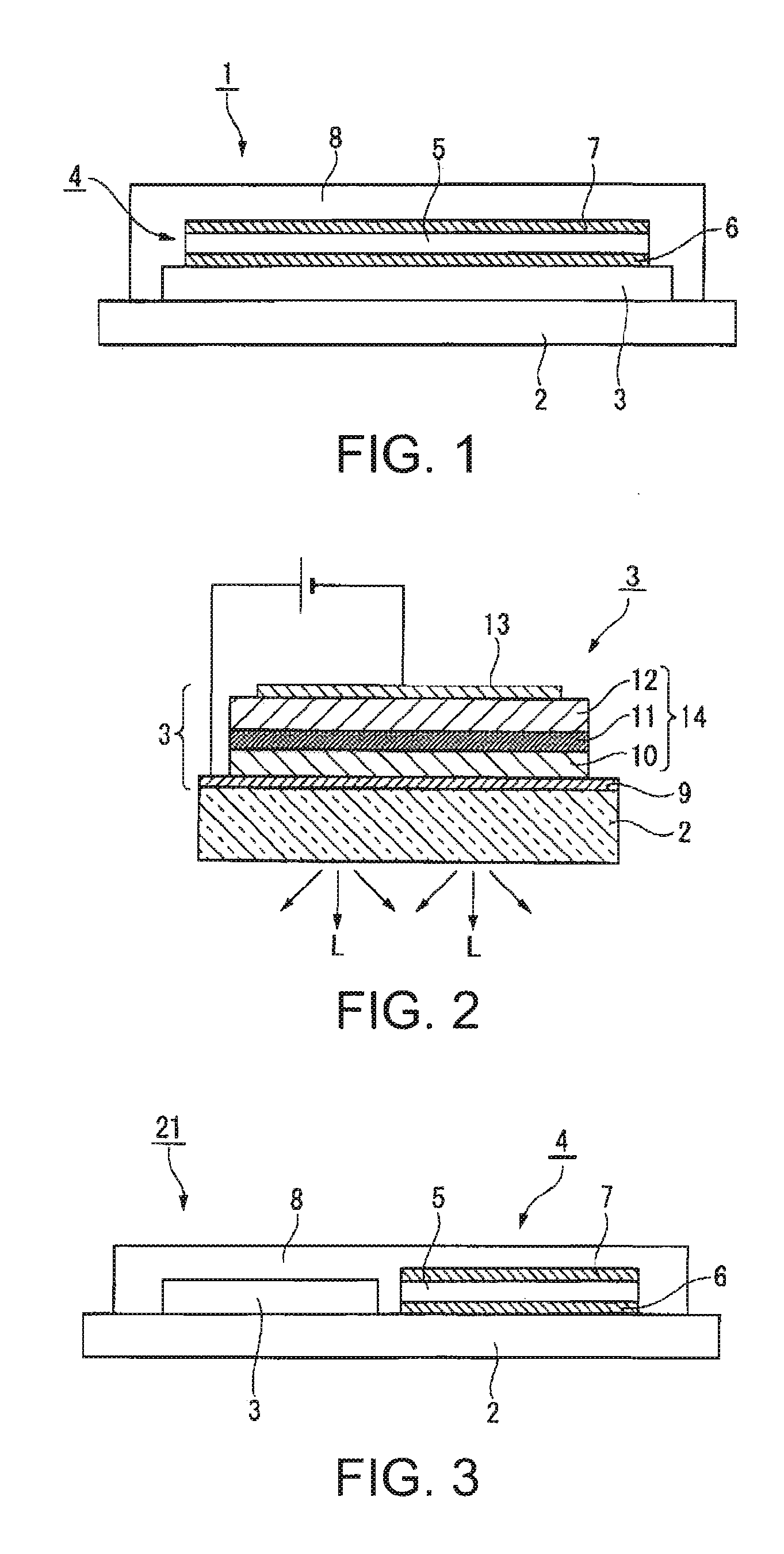
[0043] Hereinafter, a first embodiment of the invention will be explained with reference to FIGS. 1 and 2.

[0044] An organic electronic device of the present embodiment is an example of an organic EL device having an electrolytic element stacked on an organic EL element as a functional element.

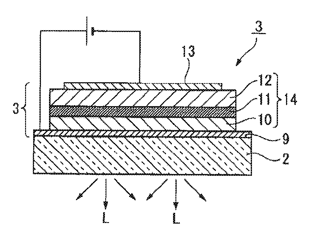
[0045]FIG. 1 is a cross-sectional view of the organic EL device according to the present embodiment, and FIG. 2 is an enlarged cross-sectional view showing a detailed configuration of an organic EL substrate. It should be noted that in all of the following drawings, the scale ratios of respective sizes and film thicknesses are set differently for every configuration element so that each of the configuration elements can be viewed easily.

[0046] As shown in FIG. 1, the organic EL device 1 according to the present embodiment provided with an organic EL element 3 formed on one surface of a glass substrate 2, and an electrolytic element 4 stacked on the organic EL element 3. The electrolytic elem...

second embodiment

[0060] Hereinafter, a second embodiment of the invention will be described with reference to FIG. 3.

[0061] An organic electronic device of the present embodiment is an example of an organic EL device having an organic EL element as a functional element and an electrolytic element disposed in parallel to each other on a substrate.

[0062]FIG. 3 is a cross-sectional view of the organic EL device according to the present embodiment. Further, in FIG. 3, the elements common to those shown in FIG. 1 are provided with the same reference numerals, and detailed explanations therefor are omitted.

[0063] As shown in FIG. 3, the organic EL device 21 according to the present embodiment provided with an organic EL element 3 formed on one surface of a glass substrate 2, and an electrolytic element 4 formed adjacent to the organic EL element 3. The cathode 6 of the electrolytic element 4 is disposed on the side of the glass substrate 2, and the anode 7 thereof is disposed on the side opposite to th...

third embodiment

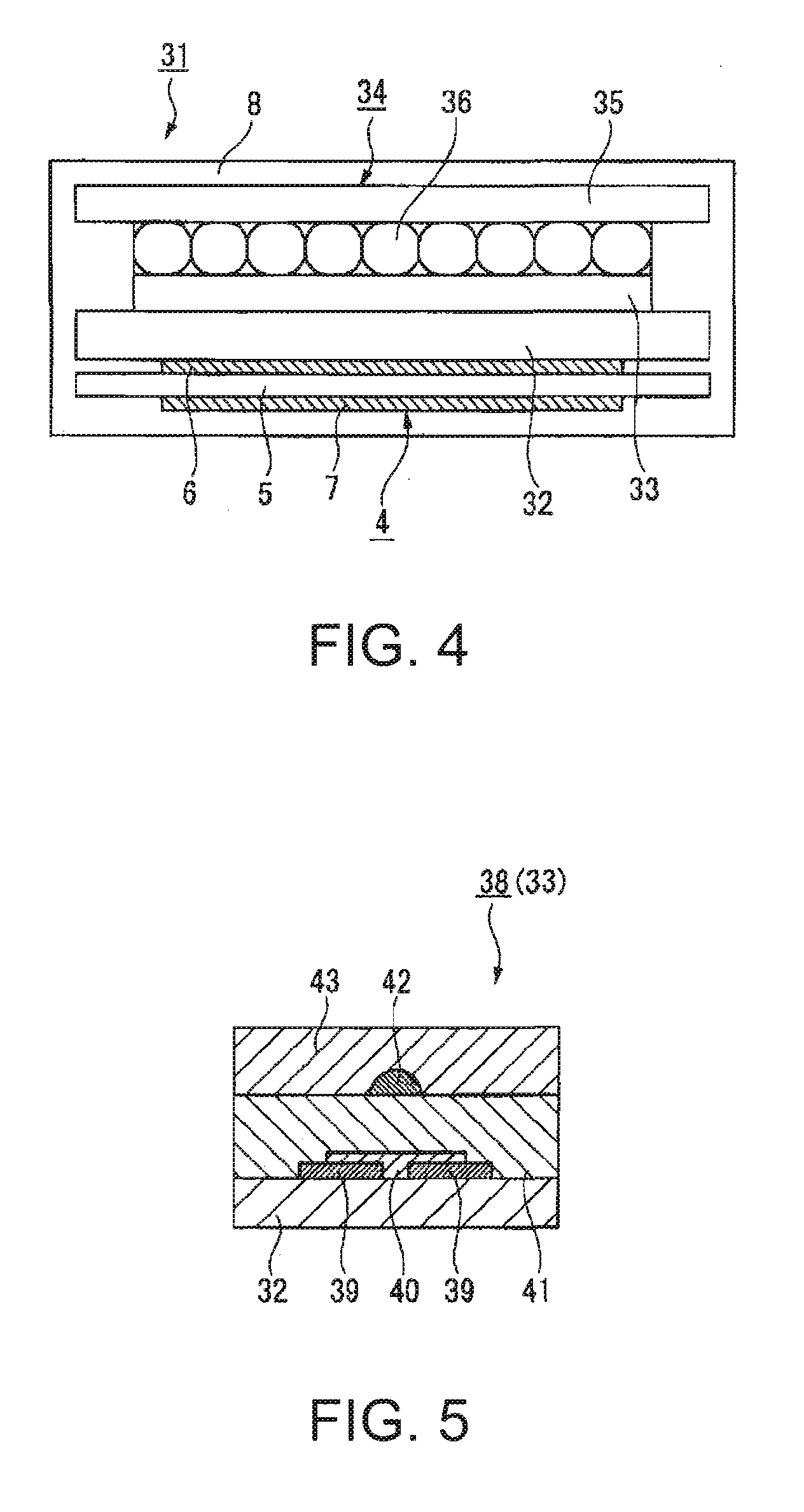
[0066] Hereinafter, a third embodiment of the invention will be described with reference to FIGS. 4 through 6.

[0067] An organic electronic device according to the present embodiment is an example of an electrophoretic display device having an organic TFT as a functional element and an electrophoretic element driven by the organic TFT both formed on one surface of the substrate and the electrolytic element formed on the other surface thereof respectively.

[0068]FIG. 4 is a cross-sectional view of the electrophoretic display device according to the present embodiment, FIG. 5 is a cross-sectional view only showing a part of the organic TFT, and FIG. 6 is a cross-sectional view of a modified example of the electrophoretic display device of the same. Further, in FIGS. 4 through 6, the elements common to those shown in FIG. 1 are provided with the same reference numerals, and detailed explanations therefor are omitted.

[0069] As shown in FIG. 4, the electrophoretic display device 31 of t...


PUM

PropertyMeasurementUnit
voltageaaaaaaaaaa
voltageaaaaaaaaaa
voltageaaaaaaaaaa

Abstract

An electronic device includes a substrate, a functional element formed on the substrate, an electrolytic element provided on at least one of a side of the substrate on which the functional element is formed and a side of the substrate opposite to the side on which the functional element is formed, configured including a solid-state electrolyte layer and a pair of electrodes for holding the solid-state electrolyte layer in between, and capable of applying electrolysis to water, and a sealing member for sealing the functional element and the electrolytic element.

Description

[0001] The entire disclosure of Japanese Patent Application No. 2006-261997, filed Sep. 27, 2006 is expressly incorporated by reference herein. BACKGROUND OF THE INVENTION [0002] 1. Technical Field [0003] The present invention relates to an electronic device, an organic electroluminescence device, and an organic thin film semiconductor device, and in particular to a sealing technology for an electronic device equipped with an organic semiconductor element, an oxide semiconductor element, or an organic electroluminescence element. [0004] 2. Related Art [0005] In recent years, portable equipment such as a mobile phone or a PDA, or a personal computer using a low profile display such as an organic electroluminescence (hereinafter also referred to simply as EL) display device or an electrophoretic display device as a display section thereof has been developed. An organic EL display device is provided with a number of light emitting elements on the surface of the substrate, and performs ...

Claims


Application Information

Patent Timeline
Patent Type & Authority Applications(United States)
IPC IPC(8): H01L51/54C25B9/00
CPCH01L27/3225H01L51/5259H01L51/5237H10K59/00H10K50/846H10K50/844H10K50/84
Inventor KAWASE, TAKEO
Owner SEIKO EPSON CORP
Why Eureka
Try Eureka