
Plasma display panel (PDP)

Inactive Publication Date: 2008-05-15
SAMSUNG SDI CO LTD
View PDF7 Cites 4 Cited by
  • Summary
  • Abstract
  • Description
  • Claims
  • Application Information

AI Technical Summary

Benefits of technology

[0011]An exemplary embodiment of the present invention provides a Plasma Display Panel (PDP) that prevents a halation effect and reduction in brightness, decreases external light reflection brightness, and improves a bright room contrast ratio to thereby realize a high-quality image.

Problems solved by technology

However, the methods of optionally shielding or coloring part of the PDP not only reduce reflection of external light but also block light emitted from the inside of the PDP to thereby deteriorate color purity and bright room contrast ratio, which is undesirable.
Moreover, when the PDP is optionally colored, the color representation on the display surface becomes blurry, which is a larger problem than the external light reflection.
Therefore, the conventional methods have a problem in that they reduce the brightness and / or the bright room contrast ratio of the PDP overall.
The method, however, brings about a drastic deterioration in the brightness of the PDP, causes blots on the dielectric layer of an upper substrate, and makes it difficult to design a cell structure.

Method used


Image

  • Plasma display panel (PDP)
  • Plasma display panel (PDP)
  • Plasma display panel (PDP)

Examples


example 1

Fabrication of a Rear Panel

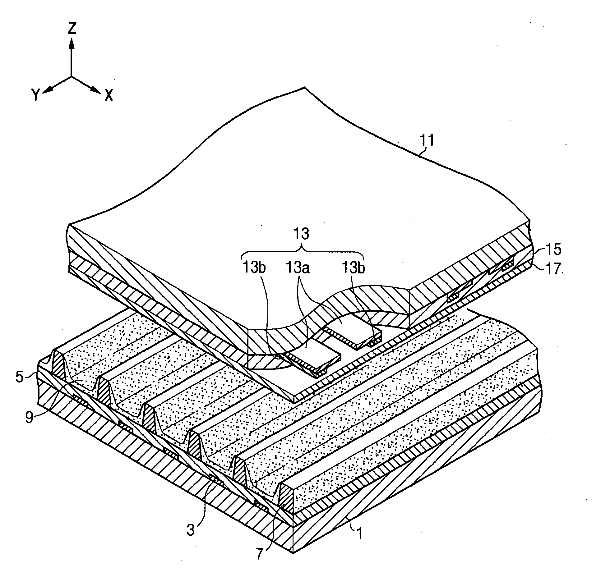
[0079]Address electrodes were formed by coating a rear substrate formed of soda lime glass with silver (Ag) paste and patterning the rear substrate. Subsequently, the entire surface of the rear substrate with the address electrodes formed thereon was coated with a dielectric layer forming composition and fired to thereby form a brown-colored dielectric layer.

[0080]Barrier ribs were formed of a glass composition on the dielectric layer. Subsequently, a red phosphor layer was formed of (Y, Gd)BO3:Eu, a blue phosphor layer was formed of BaMgAl10O17:Eu, and a green phosphor layer was formed of ZnSiO4:Mn in a region partitioned by the barrier ribs to thereby complete the fabrication of the rear panel.

[0081]Fabrication of a Front Panel

[0082]Display electrodes including indium tin oxide transparent electrodes and silver bus electrodes were formed in the shape of stripes in a conventional method on the front substrate formed of soda lime glass. Subsequently, the e...

example 2

[0087]A barrier rib forming composition was prepared by mixing a non-lead glass composition including ZnO at 10 wt %, SiO2 at 8.0 wt %, B2O3 at 22 wt %, Al2O3 at 3 wt %, Na2O at 0.5 wt %, K2O at 0.5 wt %, Li2O at 0.5 wt %, CaO at 1.0 wt %, BaO at 1.0 wt %, MgO at 1.0 wt %, SrO at 1.0 wt %, 9 ZrO2 at 5.0 wt %, and Bi2O3 at 45.5 wt %; and a coloring pigment composition including TiO2 at 0.5 wt % and CuCr2O2 at 0.5 wt %.

[0088]Ethylcellulose was used as a binder, and a-terpineol was used as a solvent. A substrate was coated with the barrier rib forming composition to a thickness of 500 μm, dried, fired at 550° C., and etched to thereby form barrier ribs.

[0089]A PDP was fabricated in the same method as in Example 1, except that the barrier rib forming composition of the above-described composition was used.

experimental example 1

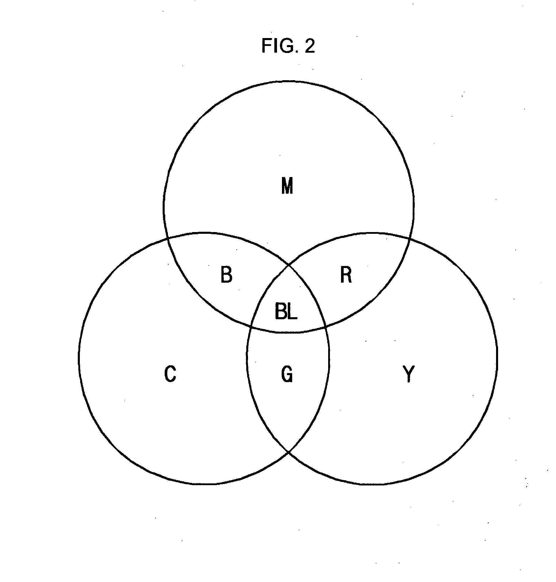
[0093]The CIE L*a*b* values of the dielectric layer and barrier ribs of the front panels fabricated according to Examples 1 and 2 and Comparative Examples 1 and 2 were measured and are presented in the following Table 1.

TABLE 1ComparativeComparativeExample 1Example 2Example 1Example 2DielectricL*a*b*L = 72L = 72L = 72L = 72layera* = 0.5a* = 0.5a* = 0.1a* = 0.1b* = −3.0b* = −3.0b* = −6.0b* = −6.0ColorBlueBlueWhiteWhiteBarrier ribL*a*b*L = 82L = 45L = 82L = 45a* = −2.0a* = 1.5a* = −2.0a* = 1.5b* = −2.0b* = 2.0b* = −2.0b* = 2.0ColorWhiteBrownWhiteBrown


PUM


Abstract

A Plasma Display Panel (PDP) includes: a first substrate and a second substrate that are arranged in parallel with each other with a predetermined distance therebetween; a plurality of address electrodes arranged on the first substrate; a first dielectric layer arranged to cover the address electrodes; a plurality of barrier ribs having a predetermined height from the first dielectric layer to define discharge cells; red, blue, and green phosphor layers respectively arranged in the discharge cells; a plurality of display electrodes arranged on one side of the second substrate facing the first substrate in a direction crossing the address electrodes; a second dielectric layer arranged to cover the display electrodes; and a protective layer arranged to cover the second dielectric layer. The second dielectric layer satisfies values of CIE L*a*b* where 70.0<L*<74.5, 0.0<a*<1.0, and −5.0<b*<−8.0.

Description

CLAIM OF PRIORITY[0001]This application makes reference to, incorporates the same herein, and claims all benefits accruing under 35 U.S.C. § 119 from an application for PLASAMA DISPLAY PANEL earlier filed in the Korean Intellectual Property Office on 9 Nov. 2006 and there duly assigned Serial No. 10-2006-0110723.BACKGROUND OF THE INVENTION[0002]1. Field of the Invention[0003]The present invention relates to a Plasma Display Panel (PDP). More particularly, the present invention relates to a PDP that prevents a halation effect and deterioration in brightness, decreases external light reflection brightness, and improves a bright room contrast ratio to thereby realize a high-quality image.[0004]2. Description of the Related Art[0005]A Plasma Display Panel (PDP) is a flat display device using a plasma phenomenon, which is also called a gas-discharge phenomenon since a discharge occurs in the panel when a potential greater than a certain level is supplied to two electrodes separated from ...

Claims


Application Information

Patent Timeline
IPC IPC(8): H01J17/49H01J11/12H01J11/38
CPCH01J11/12H01J2211/444H01J11/38H01B3/08
Inventor CHOO, SEONG-HUN
Owner SAMSUNG SDI CO LTD
Features
  • Generate Ideas
  • Intellectual Property
  • Life Sciences
  • Materials
  • Tech Scout
  • Unparalleled Data Quality
  • Higher Quality Content
  • 60% Fewer Hallucinations
Learn More