

RF tag and method of manufacturing the RF tag
a technology of rf tags and rf tags, which is applied in the direction of resonant antennas, burglar alarm mechanical actuation, instruments, etc., can solve the problems of large limitation in the type of objects to which the rf tag is attached, and the inability to provide power by itself, so as to reduce the size of the rf tag
- Summary
- Abstract
- Description
- Claims
- Application Information
AI Technical Summary
Benefits of technology
Problems solved by technology
Method used
Image

Examples
first embodiment
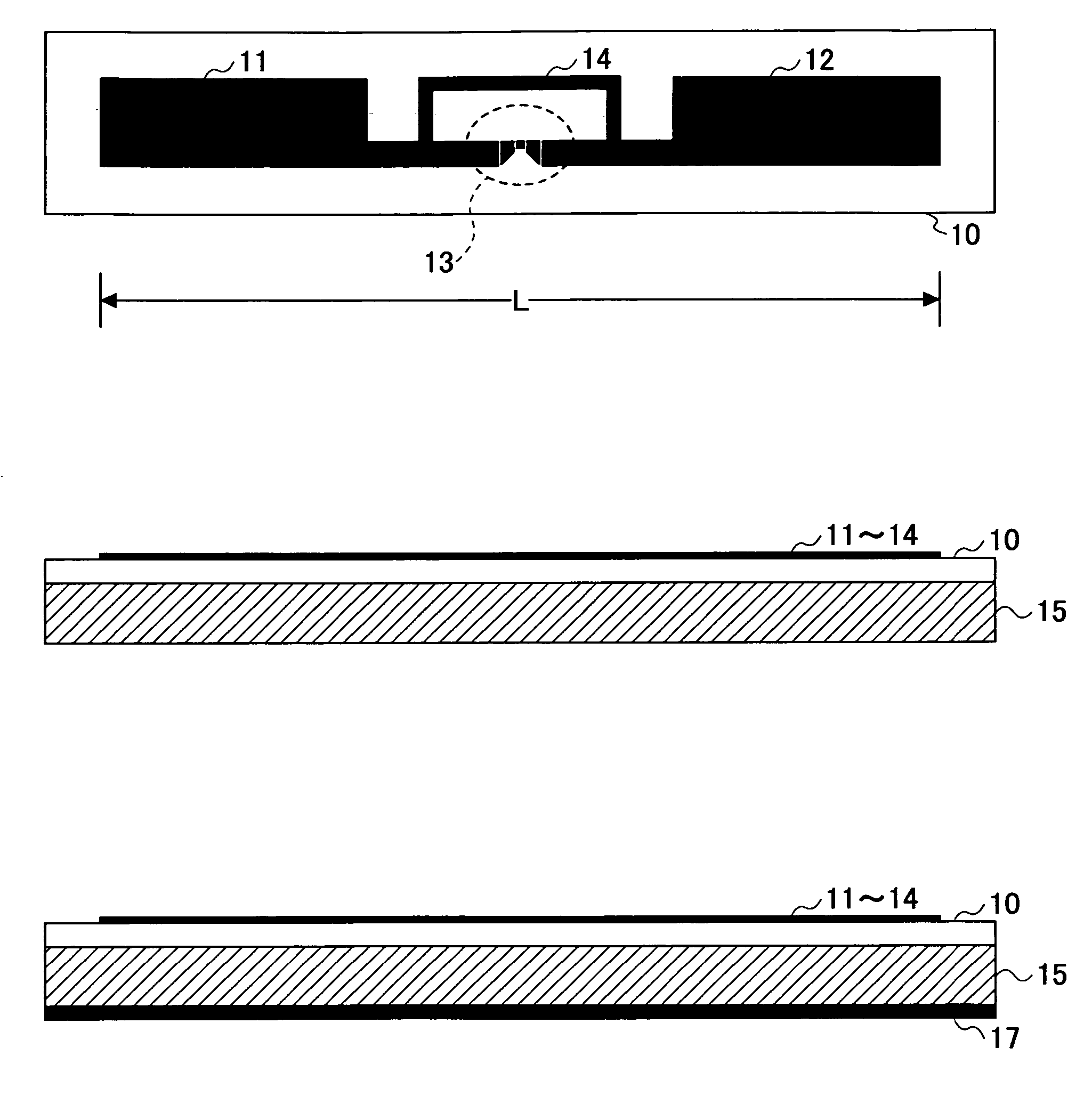
[0070]FIGS. 1A through 1C show an RF tag according to one embodiment of the present invention. FIG. 1A shows a plan view of the RF tag. FIG. 1B shows a side view of the RF tag. As graphically illustrated, the RF tag includes an insulating spacer 15, an insulating film 10 attached to the spacer 15, and an antenna pattern formed on the insulating film 10.
[0071] The spacer 15 has a thickness of, for example, several mm, and has a predetermined relative dielectric constant such as 2.3. The RF tag is attached to a conductive object (not graphically illustrated), and the object is attached to the bottom surface (a surface on the side on which the insulating film 10 is not attached) of the spacer 15. Examples of the conductive object may include any appropriate conductive articles such as the enclosure of a personal computer, steel office supplies, and steel frame materials at construction sites. The surface of the conductive object may not have sufficiently high electrical conductivity. ...
example simulation 1
[0076]FIGS. 8A through 8D show an example simulation of the antenna characteristics of an RF tag according to the present invention. FIG. 8A shows assumed antenna dimensions. It is assumed that an antenna having such dimensions is formed on a spacer of vertically 11 mm, horizontally 79 mm (in the lateral directions in the drawing), and (t) mm thick. The effect by the PET film 10 is omitted for simplification. It is assumed that the overall length of the antenna is 73 mm and the thickness of the antenna pattern is 35 μm. Further, it is assumed that the spacer has a relative dielectric constant of 2.3 and a dielectric loss (tan δ) of 2×10⁻⁴. As shown in FIG. 8A, an inductor is formed to have rectangular dimensions of vertically 5 mm and horizontally (s2) mm with a line width of 1 mm. For convenience, s2 is referred to as inductor length.
[0077] The three graphs shown in FIG. 8B show the relationship between chip capacitance CCP and the inductor length s2 with respect to spacer thickne...
example simulation 2
[0083]FIG. 10A shows assumed antenna dimensions. It is assumed that an antenna having such dimensions is formed on a spacer of vertically 11 mm, horizontally 79 mm (in the lateral directions in the drawing), and (t) mm thick. It is assumed that the thickness of the antenna pattern is 35 μm. Further, it is assumed that the spacer has a relative dielectric constant of 2.3 and a dielectric loss (tan δ) of 2×10⁻⁴. As shown in FIG. 10A, the inductor has a line width of 1 mm and rectangular dimensions of vertically 5 mm and horizontally (s2) mm. These specifications are the same as those shown in FIG. 8A, but there is a difference in that the overall length of the antenna is reduced to 63 mm.
[0084] The three graphs of FIG. 10B show the relationship between the chip capacitance CCP and the inductor length s2 with respect to spacer thicknesses t of 1, 2, and 3 mm. The three graphs of FIG. 10C show the relationship between the antenna gain (dBi) and the inductor length s2 with respect to sp...
PUM
 Abstract
Description
Claims
Application Information