Memory with a core-based virtual ground and dynamic reference sensing scheme

a dynamic reference sensing and memory technology, applied in static storage, digital storage, instruments, etc., can solve the problems of high cost and loss of data storage density, high electric power consumption, and the fundamental physical size limit of silicon-based devices

Inactive Publication Date: 2008-05-22
INFINEON TECH LLC
View PDF18 Cites 8 Cited by
  • Summary
  • Abstract
  • Description
  • Claims
  • Application Information

AI Technical Summary

Benefits of technology

[0014] The present invention disclosed and claimed herein, in one aspect thereof, comprises a method for placement of dynamic referencing circuitry internal to the chip, that is, with the core circuitry such that referencing can be performed dynamically among a number of different multi-bit reference pairs of the core that more accurately represent the reference voltage of the core. The invention includes placing the voltage reference cells in the core and cycling the reference voltage cells along with the data cells such that the effects of aging on the reference voltage is significantly reduced.

Problems solved by technology

However, silicon-based devices are approaching their fundamental physical size limits.
Inorganic solid-state devices are generally encumbered with a complex architecture that leads to high cost and a loss of data storage density.
The volatile semiconductor memories based on inorganic semiconductor material must constantly be supplied with electric current with a resulting heating and high electric power consumption in order to maintain stored information.
Non-volatile semiconductor devices have a reduced data rate and relatively high power consumption and large degree of complexity.
Techniques that have been developed with conventional single bit flash memory devices do not work well for the new multiple bit flash memory cells.
However, the buildup of charge and leakage in one bit does effect the other bit changing the reading, programming and erase characteristics of the cell in subsequent cycles.
One significant problem with dual bit operation is a result of a shift in a blank read current of the complimentary bit when the normal bit is programmed and a shift in the blank read current in the normal bit when the complimentary bit is programmed.
Another problem is caused by charge loss after cycling of the cell.
Therefore, a major challenge for dual bit operation manifests from the combination of the charge loss and complimentary bit disturb under the two conditions: (1) CBD at BOL (beginning of life) and (2) charge loss post cycling at EOL (end of life or post bake).
However, multi-bit architecture introduces an additional level of complexity related to voltage margins when determining whether a bit is in a high state or a low state.

Method used


Image

  • Memory with a core-based virtual ground and dynamic reference sensing scheme
  • Memory with a core-based virtual ground and dynamic reference sensing scheme
  • Memory with a core-based virtual ground and dynamic reference sensing scheme

Examples


Embodiment Construction

[0032] The present invention is now described with reference to the drawings, wherein like reference numerals are used to refer to like elements throughout. In the following description, for purposes of explanation, numerous specific details are set forth in order to provide a thorough understanding of the present invention. It may be evident, however, that the present invention may be practiced without these specific details. In other instances, well-known structures and devices are shown in block diagram form in order to facilitate describing the present invention.

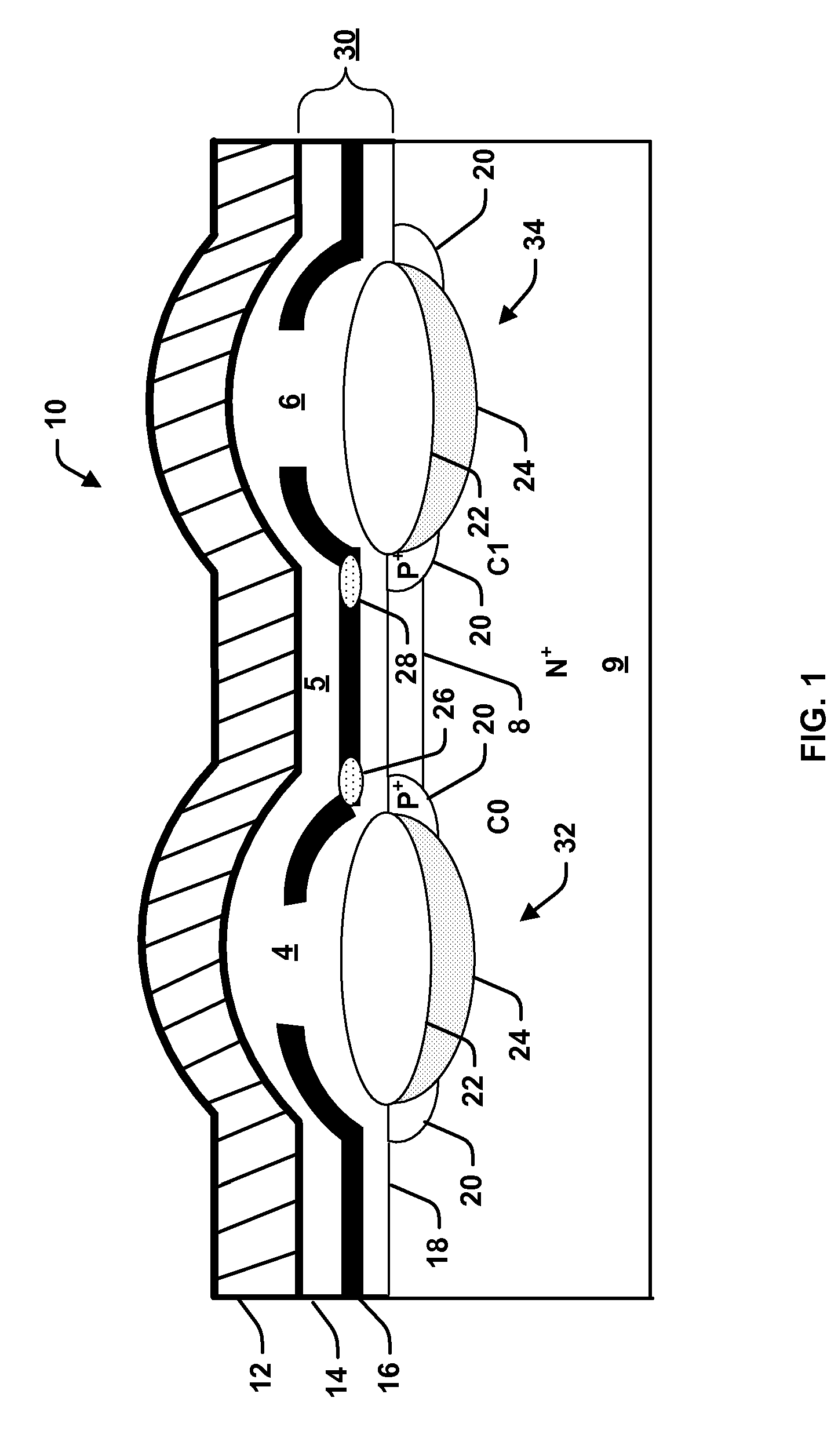
[0033] Referring now to FIG. 1, there is illustrated an exemplary dual bit memory cell 10 in which one or more of the various aspects of the invention may be carried out. The memory cell 10 comprises a silicon nitride layer 16 sandwiched between a top silicon dioxide layer 14 and a bottom silicon dioxide layer 18 forming an ONO layer 30. A polysilicon layer 12 resides over the ONO layer 30 and provides a wordline connec...


PUM


Abstract

A core-based multi-bit memory (400) having a dual-bit dynamic referencing architecture (408, 410) fabricated on the memory core (401). A first reference array (408) and a second reference array (410) are fabricated on the memory core (401) such that a reference cell pair (185) comprising one cell (182) of the first reference array (408) and a corresponding cell (184) of the second reference array (410) are read and averaged to provide a reference voltage for reading a data array(s).

Description

CROSS REFERENCE TO RELATED APPLICATIONS [0001] This application is a continuation of U.S. patent application Ser. No. 10 / 600,065, filed on Jun. 20, 2003, entitled “MEMORY WITH A CORE-BASED VIRTUAL GROUND AND DYNAMIC REFERENCE SENSING SCHEME”, the entirety of which is incorporated herein by reference.TECHNICAL FIELD [0002] This invention is related to multi-bit chip memory, and more specifically, to methods and systems for on-chip placement of referencing circuitry in a multi-bit memory device. BACKGROUND OF THE INVENTION [0003] The use of portable computer and electronic devices has greatly increased demand for memory devices. Digital cameras, digital audio players, personal digital assistants, and the like generally seek to employ large capacity memory devices (e.g., flash memory, smart media, compact flash, . . . ). The increased demand for information storage is commensurate with memory devices having an ever-increasing storage capacity (e.g., increase storage per die or chip). A...

Claims


Application Information

Patent Timeline
Patent Type & Authority Applications(United States)
IPC IPC(8): G11C16/04G11C16/06G11C11/56G11C16/28
CPCG11C11/5642G11C11/5671G11C2211/5634G11C16/28G11C16/0475G11C5/14G11C7/00G11C11/56
Inventor SHIEH, MING-HUEIKURIHARA, KAZUHIRO
Owner INFINEON TECH LLC
Why Eureka
Try Eureka