Phase-change memory

A phase-change memory and phase-change memory technology, which is applied in the field of memory and phase-change memory, can solve problems such as difficult DUMMY resistance, data storage error, and resistance value reduction, so as to reduce the read operation voltage or current, and reduce the chip area , The effect of reducing process deviation

Active Publication Date: 2008-12-31
SHANGHAI INST OF MICROSYSTEM & INFORMATION TECH CHINESE ACAD OF SCI
View PDF0 Cites 7 Cited by
  • Summary
  • Abstract
  • Description
  • Claims
  • Application Information

AI Technical Summary

Problems solved by technology

[0006] There are many problems in the 1D1R memory with this traditional structure: First, due to the process deviation and the unequal distance between the memory cell and the drive circuit in the chip layout, the resistance value distribution of the phase change unit in the "RESET" and "SET" states is different. Wider, even the phenomenon that the resistances in the two states overlap, resulting in data storage errors
Second, because the read operation requires a pulse signal, the phase change in 1R1D will continue to decrease with the accumulation of the read pulse signal after multiple read operations. When the resistance value under "RESET" is smaller than the DUMMY resistance, Data read errors will be released, and this phenomenon will be more serious if a higher read operation voltage or a higher read operation current is used
Third, because the resistance value of the phase-change memory cell will become very complicated after multiple RESET and SET operations, and the DUMMY resistance will not change accordingly, so the comparison with the DUMMY resistance will become more difficult
[0007] From the above, it can be seen that the traditional phase-change memory has the following problems to be solved: First, under the traditional 1T1R or 1D1R structure, most of the area of ​​the memory array is consumed by the MOS transistor or diode used as the gate transistor. However, it has not reached the highest integration level of the phase change unit
Second, according to the experiment, it is found that the phase change memory cells on the same phase change memory chip, due to the lack of process consistency and the different distances between the phase change cells and the driving circuit, the distribution of high resistance values ​​after RESET operation is different from the distribution of low resistance values ​​after SET. The value distribution is very wide (high resistance 20k-500kOhm, low resistance 1k-10kOhm), and even high resistance and low resistance values ​​overlap, which has a great impact on the correct reading of the data on the phase change unit, and the resistance of the circuit The interference ability is weak, and the reading speed is slow; thirdly, the phase change memory depends on Joule heat to change its resistance state. The resistance of the SET state will decrease as the number of read operations increases. Under the traditional 1T1R and 1D1R structures, when the resistance value of the phase change unit in the "RESET" state is low to a certain extent, reading errors may occur, and high and low resistance The smaller the value gap will also affect the chip read margin
Fourth, after the phase change unit is operated by multiple RESET or SET, the resistance value of the device itself will be very complicated

Method used


Image

  • Phase-change memory
  • Phase-change memory
  • Phase-change memory

Examples


Embodiment 1

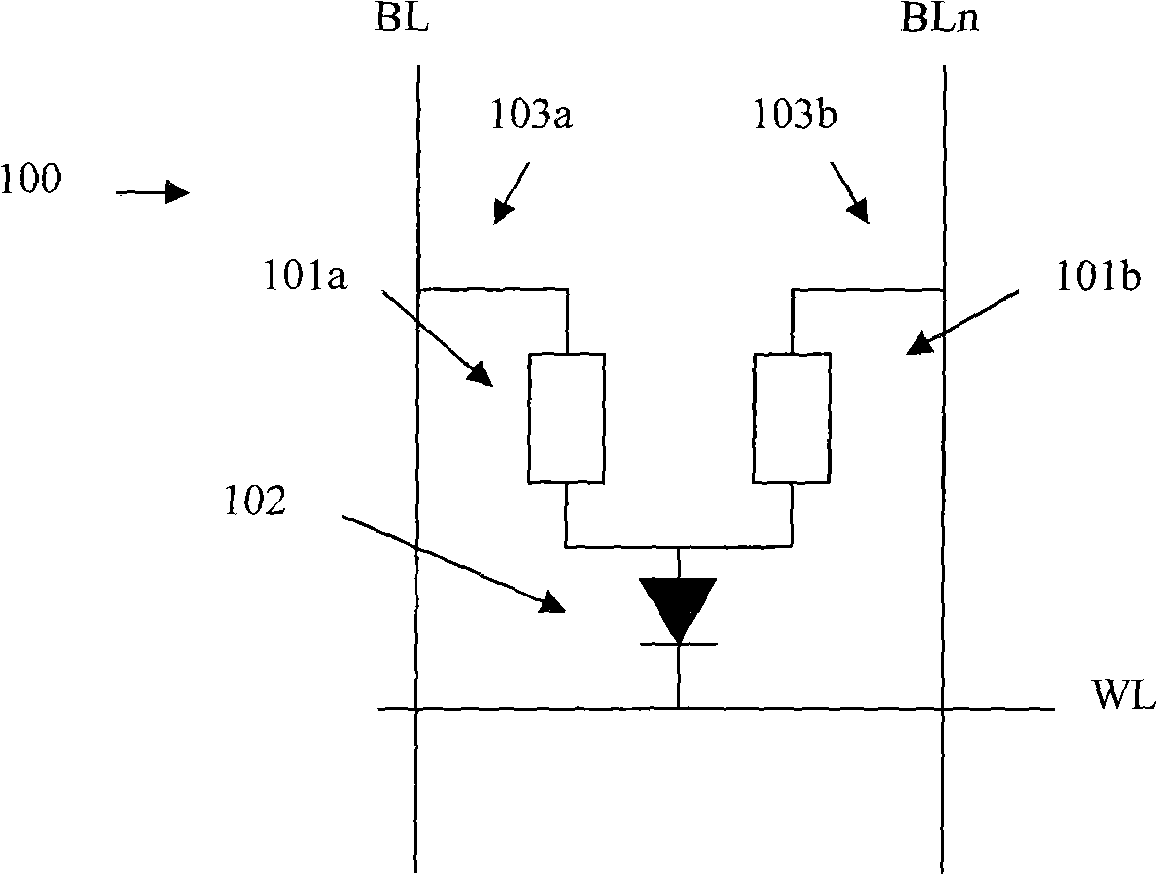
[0031]see figure 1 , figure 2 and Figure 4 , this embodiment introduces a phase change memory 400 in which the storage unit is a 1D2R structure.

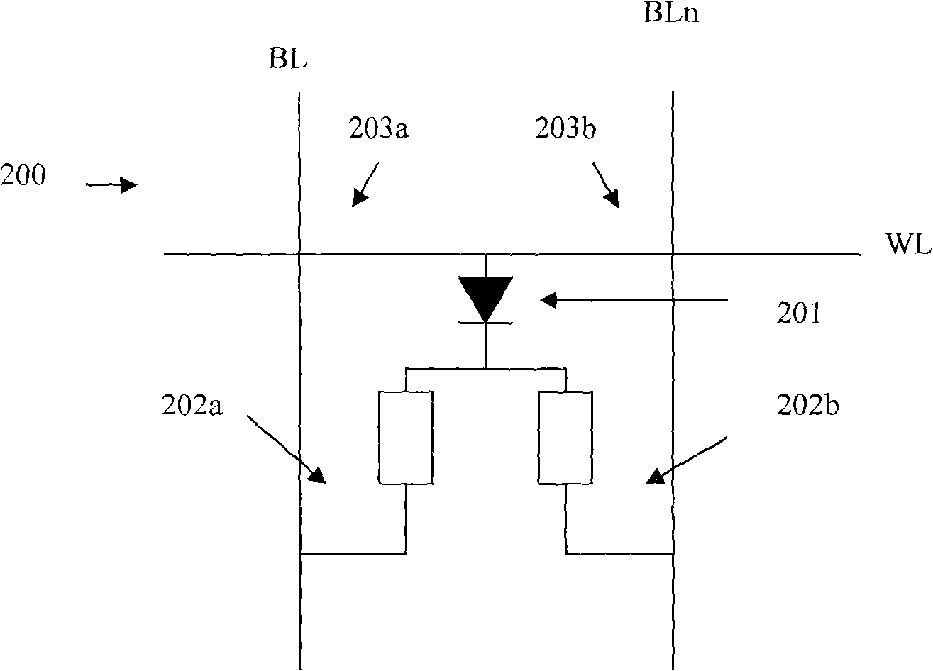
[0032] Firstly, the structure of the storage unit in this embodiment is introduced. Such as figure 1 As shown, the memory cell 100 includes phase change memory cells 101a and 101b, a gate diode 102, phase change material upper electrodes 103a and 103b, a word line WL, and bit lines BL and BLn. Wherein the phase-change memory unit 101a and the phase-change memory unit 101b store two complementary data (so in this embodiment "phase-change memory unit" can also be called "complementary state phase-change unit"), for example, when 101a is "RESET" state, 101b is in the "SET" state, that is, two phase-change units are used to store 1-bit data. In this embodiment, the phase-change memory cells 101a and 101b are connected in parallel and connected to the anode of the gate diode 102 . The storage unit can also be figure 2 The str...

Embodiment 2

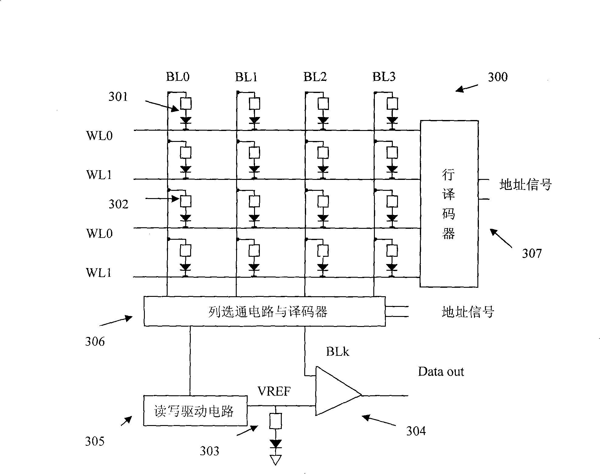
[0040] see Figure 7 , this embodiment introduces a phase change memory 700 in which the storage unit is a 1DnR structure, where n is an integer greater than or equal to 2. In a memory cell with a 1DnR structure, n phase-change resistors share a gate diode to store n-bit data.

[0041] Such as Figure 7 As shown, the present invention discloses a phase-change memory 700, including several storage units 701, a column gate circuit and a decoder 702, a read comparison resistor 703, a sense amplifier 704, a read-write drive circuit 705, and a row decoder 706 . The bit line of each memory cell 701 is connected to the column gate circuit and decoder 702, and the word line of each memory cell 701 is connected to the row decoder 706; the column gate circuit and decoder 702 is connected to the read-write drive circuit 705 and the sense amplifier 704 , and the read-write drive circuit 705 is connected to the sense amplifier 704 through the read comparison resistor 703 . The column g...

Embodiment 3

[0045] The difference between this embodiment and Embodiment 2 is that in this embodiment, the number of phase-change memory cells of each memory cell is different or not completely the same. Its implementation principle is the same as that of Embodiment 2, and will not be repeated here.


PUM


Abstract

The invention discloses a phase-change memory which comprises a plurality of memory units, a column gating circuit, a decoder, a comparative readout resistor, a sensitive amplifier, a read-write drive circuit and a row decoder; bit lines of all the memory units are connected to the column gating circuit and the decoder; the word lines of all the memory units are connected to the row decoder; the column gating circuit and the decoder are connected with the read-write drive circuit and the sensitive amplifier; the read-write drive circuit is connected with the sensitive amplifier by the comparative readout resistance; the memory unit comprises a gating diode and at least two phase-change memory units; after being parallel, the phase-change memory units are connected with the gating diode. The phase-change memory of the invention adopts a 1DnR memory unit structure, thus reducing the chip area occupied by the gating diode.

Description

technical field [0001] The invention belongs to the technical field of semiconductor storage and relates to a memory, in particular to a phase-change memory capable of accelerating the reading speed of the memory and increasing the reading margin. Background technique [0002] Phase change memory technology is based on Ovshinsky's proposal in the late 1960s (Phys. Rev. Lett., 21, 1450-1453, 1968) and early 1970s (Appl. Phys. Lett., 18, 254-257, 1971) The idea that the phase change film can be applied to the phase change storage medium is established, and it is a storage device with low price and stable performance. Phase-change memory can be made on a silicon wafer substrate, and its key materials are recordable phase-change films, heating electrode materials, heat-insulating materials, and lead-out electrode materials. Including how to reduce device material and so on. The basic principle of phase change memory is to use electric pulse signal to act on the device unit, so...

Claims


Application Information

Patent Timeline
Patent Type & Authority Applications(China)
IPC IPC(8): G11C11/56G11C16/08
Inventor 富聪宋志棠蔡道林封松林
Owner SHANGHAI INST OF MICROSYSTEM & INFORMATION TECH CHINESE ACAD OF SCI
Why Eureka
Try Eureka