Method of Manufacturing Thin Film, Method of Manufacturing P-Type Zinc Oxide Thin Film and Semiconductor Device

a technology of zinc oxide and manufacturing method, which is applied in the direction of crystal growth process, electric/magnetic/electromagnetic heating, transportation and packaging, etc., can solve the problems of p-type conduction and p-type conduction cannot be achieved, and achieve rapid increase and decrease of temperature, and high crystallinity and surface flatness

Inactive Publication Date: 2008-05-22
TOHOKU UNIV
View PDF6 Cites 7 Cited by
  • Summary
  • Abstract
  • Description
  • Claims
  • Application Information

AI Technical Summary

Benefits of technology

[0017]According to the present invention, the doping can be performed at high concentration while maintaining high crystallinity and surface flatness by the multi-stage annealing process during the growth of the thin film. With an apparatus of manufacturing a thin film using a computer-controlled laser as a heat source, the rapid increase and decrease of the temperature which is difficult for a prior resistor heater can be performed. According to the present invention, nitrogen doping can be performed at high concentration while maintaining the high crystallinity and surface flatness of the p-type zinc oxide thin film. According to the present invention, the p-type zinc oxide single crystal thin film can be obtained.

Problems solved by technology

However, in this prior art, aiming at p-type conduction cannot be achieved because the crystallinity is not adequate.
However, in this prior art, also, aiming at p-type conduction cannot be achieved.

Method used


Image

  • Method of Manufacturing Thin Film, Method of Manufacturing P-Type Zinc Oxide Thin Film and Semiconductor Device
  • Method of Manufacturing Thin Film, Method of Manufacturing P-Type Zinc Oxide Thin Film and Semiconductor Device
  • Method of Manufacturing Thin Film, Method of Manufacturing P-Type Zinc Oxide Thin Film and Semiconductor Device

Examples


first embodiment

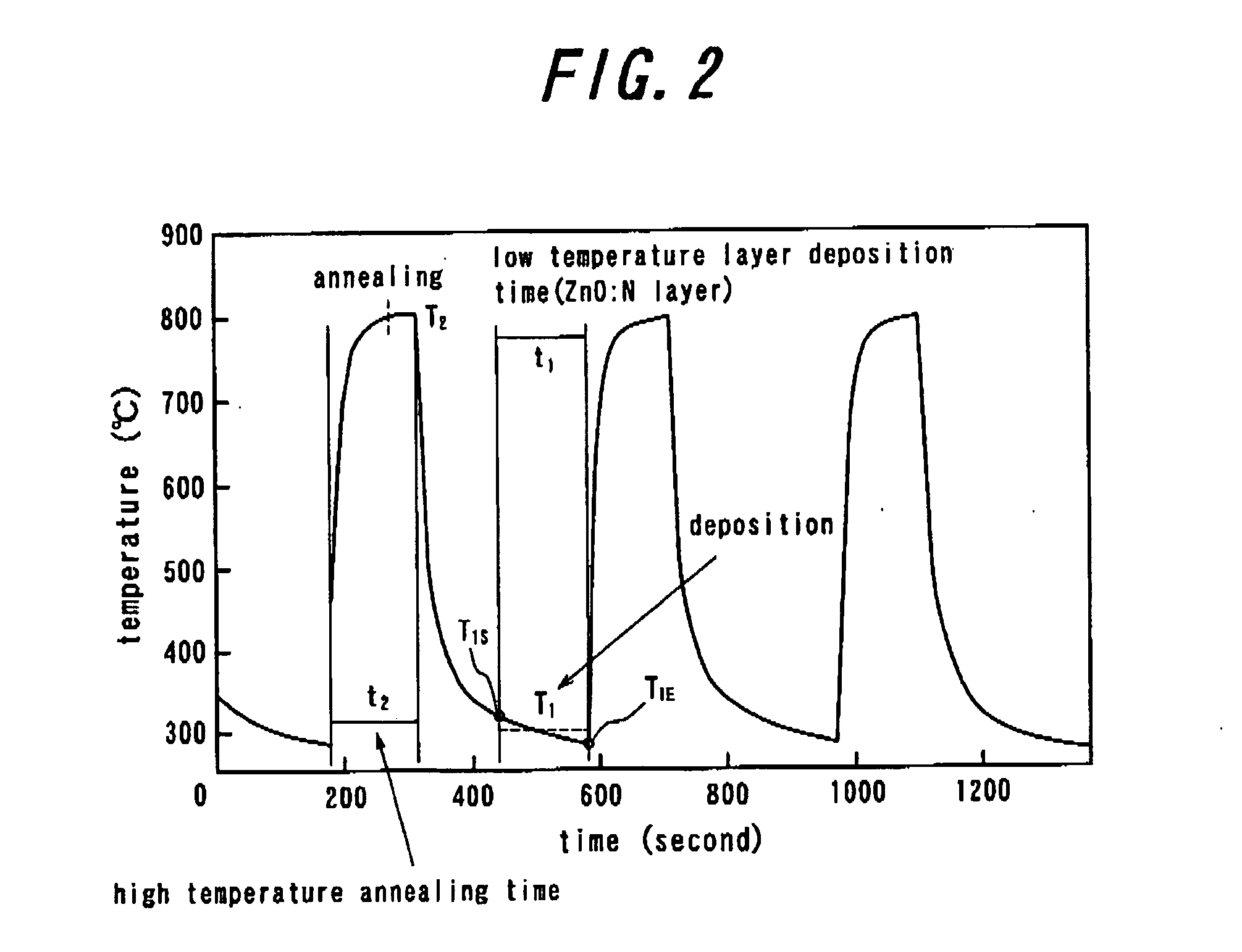
[0029]FIG. 2 is a graph showing a sequence of the growth temperature and the thin film deposition in the method of manufacturing the thin film according to the present invention. First of all, as a first step, a low temperature highly doped layer is formed by performing doping while growing a thin film at a first temperature T1 of about 300° C. during time t1. The temperature T1 is defined as an arithmetic mean of a first temperature and a last temperature at time t1. (T1=(T1S+T1E) / 2) It is advantageous to form such a low temperature highly doped layer in order to increase nitrogen concentration. Next, as a second step, the growth of the thin film is interrupted, and the temperature of the thin film is risen to a second temperature T2 of about 800° C. by irradiating the Nd:YAG laser onto the substrate holder 10 with the control of the computer 2. The second temperature is maintained during time t2 and the thin film is annealed. Such a high temperature annealing can reduce a crystal ...

second embodiment

[0031]FIG. 4 is a graph showing the nitrogen concentration measured in the zinc oxide thin film manufactured by the method according to the present invention and that manufactured by the method according to prior art performing doping at a constant growth temperature. The zinc oxide thin film comprises the low temperature highly doped layer having a thickness of 9 nm and the high temperature lowly doped layer having a thickness of 1 nm, and is manufactured by the method comprising three steps of the In this graph, the growth temperature of the zinc oxide thin film manufactured by the present invention is T1 in the temperature profile shown in FIG. 3. The zinc oxide thin film manufactured by the present invention has a higher average growth temperature than that of the zinc oxide thin film manufactured by the method according to prior art, however, the zinc oxide thin film manufactured by the present invention has high nitrogen concentration. This means that the nitrogen doped at lo...


PUM

PropertyMeasurementUnit
temperatureaaaaaaaaaa
temperature T2aaaaaaaaaa

Abstract

There is provided a method of manufacturing a thin film, in which not only high crystallinity and surface flatness can be realized but also dopant doping can be performed at high concentration. The method includes a low temperature highly doped layer growing step of performing dopant doping while growing the thin film at a given first temperature; an annealing step of interrupting the growth of the thin film and annealing the thin film at a given second temperature higher than the first temperature; and a high temperature lowly doped layer growing step of growing the thin film at the second temperature.

Description

TECHNICAL FIELD[0001]The present invention relates to a method of manufacturing a thin film. Especially, the present invention relates to a method of manufacturing a p-type zinc oxide thin film. The present invention also relates to a semiconductor device comprising a p-type zinc oxide thin film manufactured by such a method.BACKGROUND ART[0002]As a new thin film material next to III-V nitride used in ultraviolet light emitting element and so on, zinc oxide is attracted. In such zinc oxide, high crystallinity and surface flatness are required and nitrogen doping at high concentration is also required in order to aim at p-type conduction. However, in order to obtain the high crystallinity and surface flatness, it is necessary to keep high growth temperature, and in order to perform doping at the high concentration, it is necessary to keep low growth temperature. It is known that the nitrogen is activated as an acceptor in the zinc oxide, and in order to perform the doping at the high...

Claims


Application Information

Patent Timeline
Patent Type & Authority Applications(United States)
IPC IPC(8): H01L29/12B29C71/00H05B6/00C30B29/16H01L21/205H01L21/363H01L33/28
CPCH01L21/02554Y10T428/12528H01L21/02631H01L21/02579
Inventor KAWASAKI, MASASHIOHTOMO, AKIRAFUKUMURA, TOMOAKITSUKAZAKI, ATSUSHIOHTANI, MAKOTO
Owner TOHOKU UNIV
Why Eureka
Try Eureka