Group III nitride semiconductor devices and methods of making

a technology of nitride and metal oxide semiconductors, applied in the field of group iii nitride metal oxide semiconductor devices, can solve the problem that devices typically exhibit shifts in device parameters

Inactive Publication Date: 2008-05-29
GENERAL ELECTRIC CO
View PDF6 Cites 23 Cited by
  • Summary
  • Abstract
  • Description
  • Claims
  • Application Information

AI Technical Summary

Problems solved by technology

Such devices typically exhibit shifts in device parameters with temperature.

Method used


Image

  • Group III nitride semiconductor devices and methods of making
  • Group III nitride semiconductor devices and methods of making
  • Group III nitride semiconductor devices and methods of making

Examples


Embodiment Construction

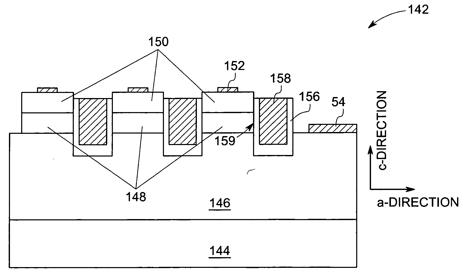
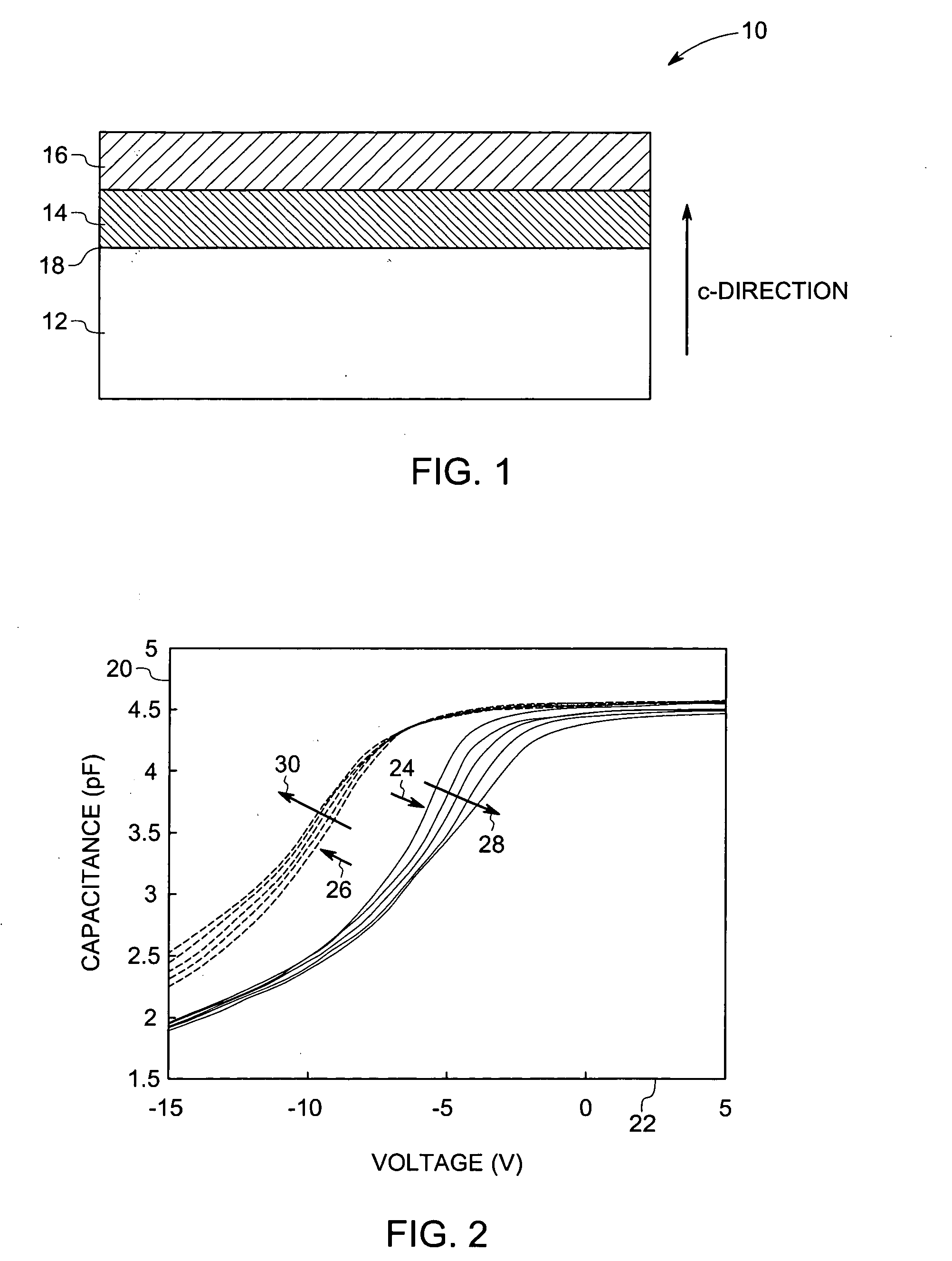
[0022]As described further below, embodiments of the present invention disclose devices including an electrode-insulator-group III nitride semiconductor layer structure, wherein the insulator-semiconductor layer interface lies along a non-polar plane of the semiconductor.

[0023]As used herein, the term “non-polar plane” refers to a plane within plus or minus 10 degrees off an ideal non-polar plane for a group III nitride.

[0024]As used herein, the terms, “oxide layer” and “insulator layer” are used interchangeably and refer to insulating layers, non-limiting examples of which include SiO2 layers. Those skilled in the art will appreciate that while the terms may be used interchangeably herein, oxide is merely one example of an insulator that may be used. An example of a non-oxide insulator layer is a SiNx layer.

[0025]As used herein, the terms, “metal-oxide-semiconductor field effect transistor (MOSFET)”, “metal-insulator-semiconductor field effect transistor (MISFET)”, “insulated gate ...


PUM

PropertyMeasurementUnit
operating temperatureaaaaaaaaaa
thickaaaaaaaaaa
thickaaaaaaaaaa

Abstract

A device having an electrode-insulator layer-group III nitride layer structure, wherein an interface between the insulator layer and the group III nitride semiconductor layer lies along a non-polar plane of the group III nitride semiconductor layer is provided.

Description

BACKGROUND[0001]The invention relates generally to group III nitride devices, and more particularly to group III nitride metal oxide semiconductor (MOS) devices.[0002]Electronic devices based on wide bandgap semiconductors offer superior high voltage, high power, high temperature, and high frequency operation. Wide band gap group III nitride semiconductor materials include but are not limited to materials such as gallium nitride, aluminum nitride, and aluminum-gallium nitride materials. For example, gallium nitride (GaN) is a semiconductor material with a wide (3.4 eV) band gap and a high (2500° C.) melting point. GaN is a hard, mechanically stable material with large heat capacity. These properties make it especially suitable for use in a high-frequency, high-power device operated at a high temperature and / or under high-voltage conditions.[0003]High-power metal-oxide-semiconductor field effect transistors (MOSFET) devices are desirable for various power electronic applications. GaN...

Claims


Application Information

Patent Timeline
Patent Type & Authority Applications(United States)
IPC IPC(8): H01L29/20H01L21/336
CPCH01L29/045H01L29/94H01L29/2003
Inventor MATOCHA, KEVIN SEANTILAK, VINAYAK
Owner GENERAL ELECTRIC CO
Why Eureka
Try Eureka