

Non-conformal stress liner for enhanced mosfet performance
- Summary
- Abstract
- Description
- Claims
- Application Information
AI Technical Summary
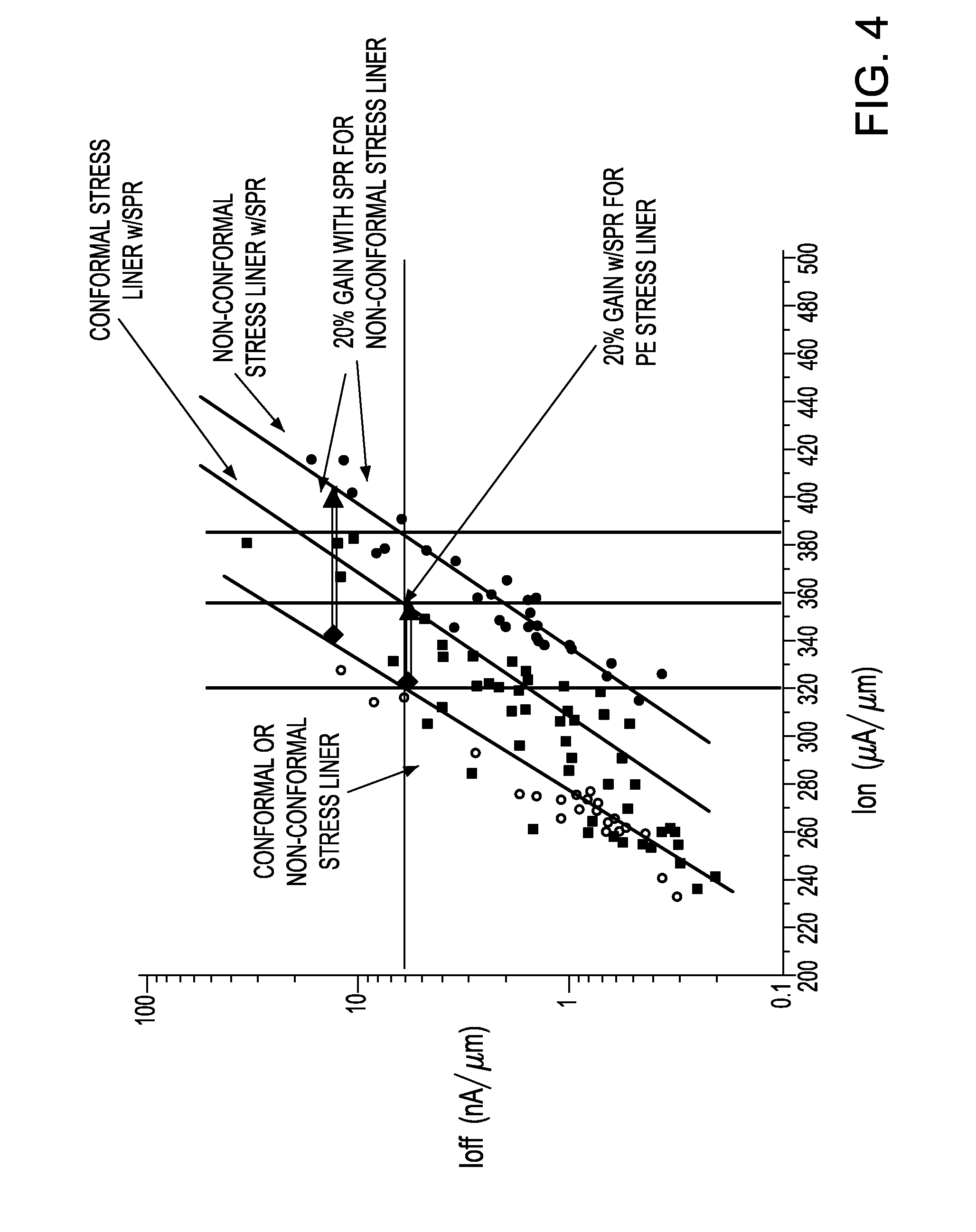
Benefits of technology
Problems solved by technology
Method used
Image

Examples
Embodiment Construction
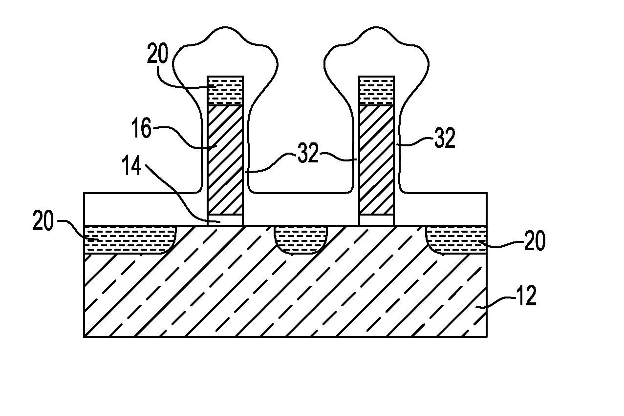
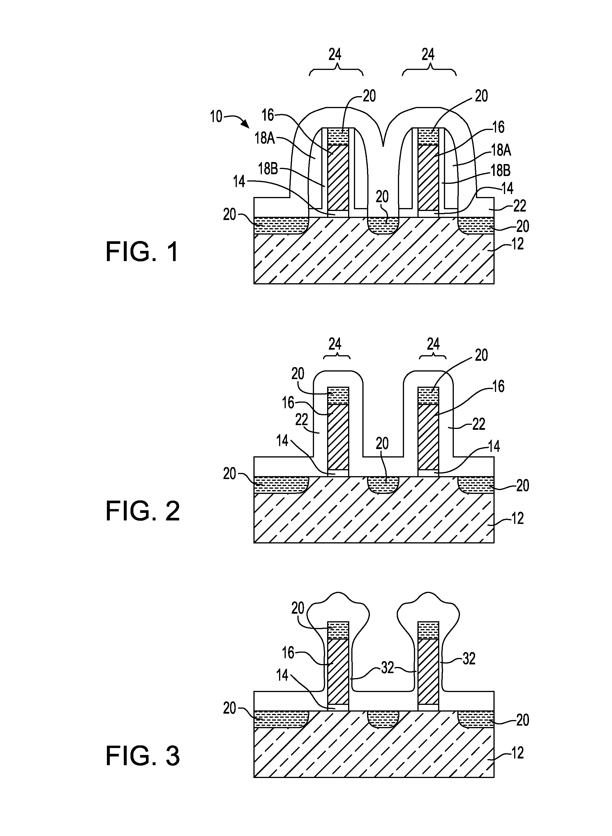
[0024]The present invention, which provides a semiconductor structure including a non-conformal stress liner that is employed together with offset spacer reduction or removal (SPR) in order to increase the mechanical stress into the device channel, will now be described in greater detail by referring to the following discussion and drawings that accompany the present application. It is noted that the drawings of the present application are provided for illustrative purposes and, as such, the drawings are not drawn to scale.
[0025]In the following description, numerous specific details are set forth, such as particular structures, components, materials, dimensions, processing steps and techniques, in order to provide a thorough understanding of the present invention. However, it will be appreciated by one of ordinary skill in the art that the invention may be practiced without these specific details. In other instances, well-known structures or processing steps have not been described...
PUM
 Abstract
Description
Claims
Application Information