

Methods of forming SRAM constructions
- Summary
- Abstract
- Description
- Claims
- Application Information
AI Technical Summary
Benefits of technology
Problems solved by technology
Method used
Image

Examples
Embodiment Construction
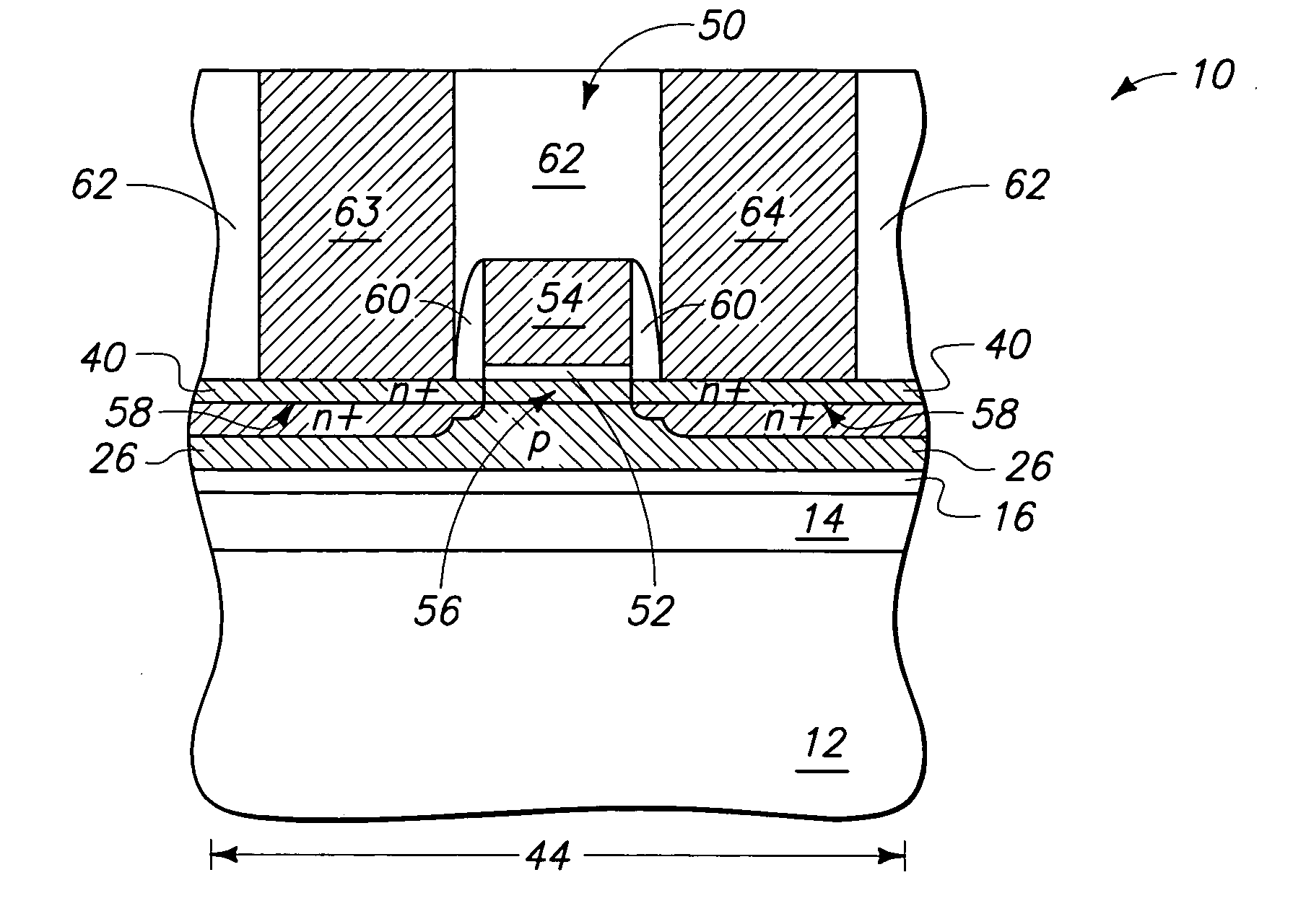
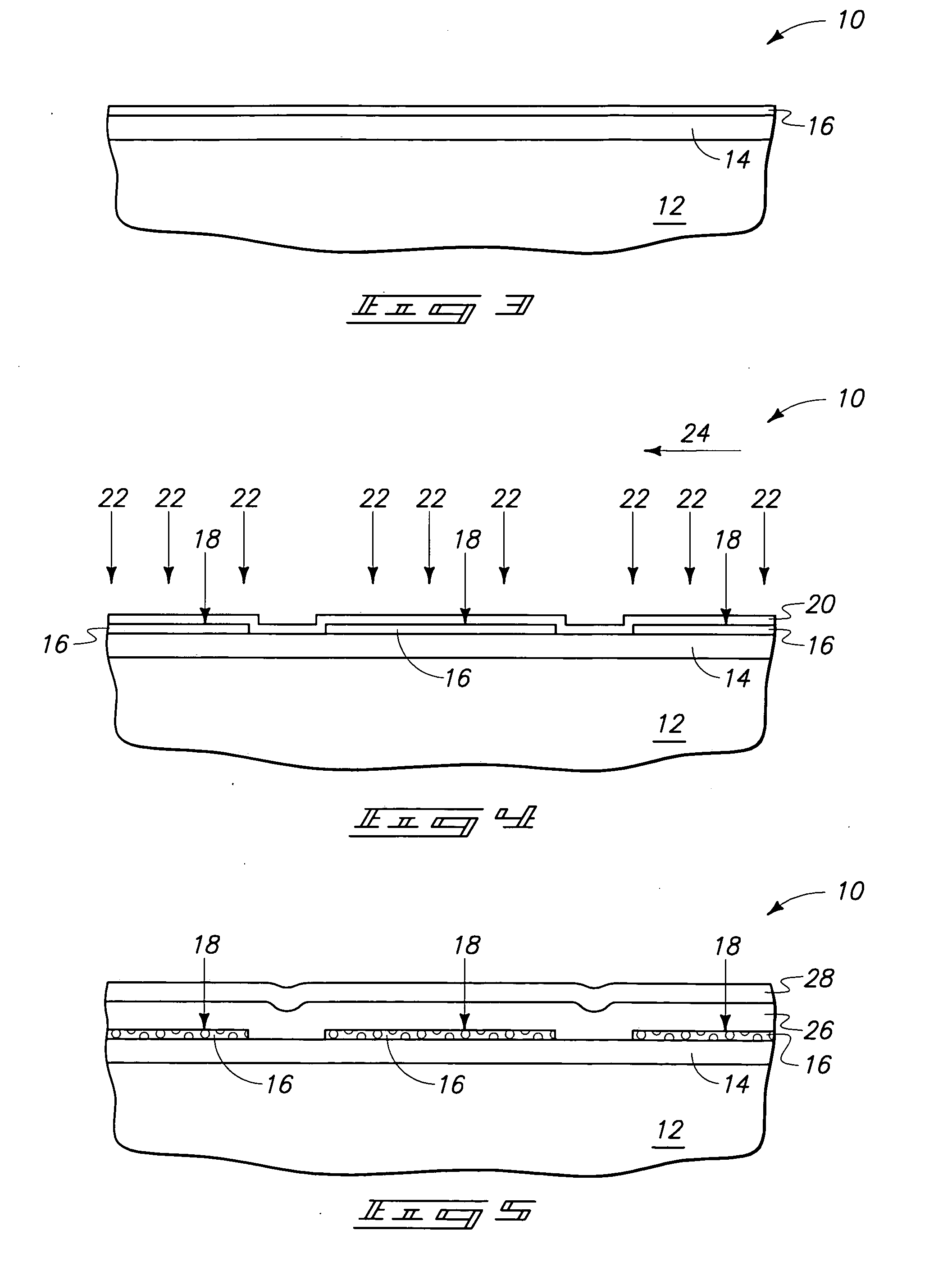
[0060] The invention pertains to SRAM devices. Prior to the discussion of the exemplary SRAM devices of the invention, processing sequences for forming and utilizing preferred Si / Ge materials are described with reference to FIGS. 3-17.
[0061] Referring to FIG. 3, a fragment of a semiconductor construction 10 is illustrated at a preliminary processing stage. To aid in interpretation of the claims that follow, the terms “semiconductive substrate” and “semiconductor substrate” are defined to mean any construction comprising semiconductive material, including, but not limited to, bulk semiconductive materials such as a semiconductive wafer (either alone or in assemblies comprising other materials thereon), and semiconductive material layers (either alone or in assemblies comprising other materials). The term “substrate” refers to any supporting structure, including, but not limited to, the semiconductive substrates described above.
[0062] Construction 10 comprises a base (or substrate) ...
PUM
 Abstract
Description
Claims
Application Information