Light-Emitting Element and Light-Emitting Device Using the Same

a technology of light-emitting devices and light-emitting elements, which is applied in the direction of discharge tube luminescnet screens, other domestic articles, natural mineral layered products, etc., can solve the problems of insufficient document 1 alone and the need for much lower driving voltage, and achieve low driving voltage and not increased driving voltage. , the effect of producing favorable yield

Inactive Publication Date: 2008-05-29
SEMICON ENERGY LAB CO LTD
View PDF22 Cites 58 Cited by
  • Summary
  • Abstract
  • Description
  • Claims
  • Application Information

AI Technical Summary

Benefits of technology

[0030]According to the present invention, a light-emitting element that is not likely to be crystallized can be obtained and a light-emitting element achieving a lower driving voltage can be obtained. In addition, even when the light-emitting element according to the present invention is made thicker, the driving voltage is not increased. Accordingly, the light-emitting element can be formed to be thicker, and can be thus produced at a favorable yield. Further, an electrode and a light-emitting layer can be kept further away from each other depending on which layer is made thicker, and quenching of luminescence can be thus prevented.
[0031]Further, the light-emitting element according to the present invention has high thermal stability and high heat resistance, which is preferable. Accordingly, the light-emitting element is less deteriorated with time.

Problems solved by technology

Therefore, the way disclosed in Patent Document 1 alone is said to be insufficient, and technologic development for achieving a much lower driving voltage has been needed.

Method used


Image

  • Light-Emitting Element and Light-Emitting Device Using the Same
  • Light-Emitting Element and Light-Emitting Device Using the Same
  • Light-Emitting Element and Light-Emitting Device Using the Same

Examples


embodiment 1

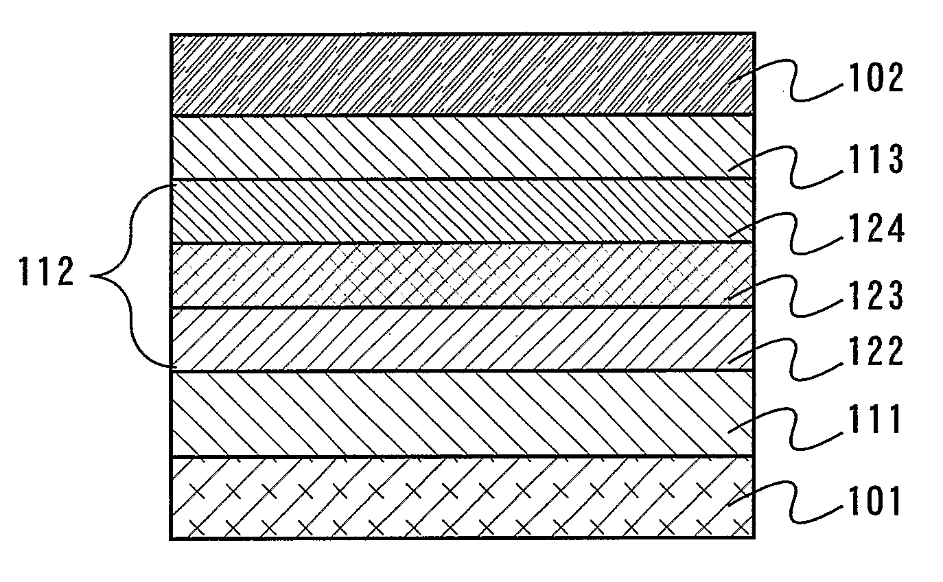
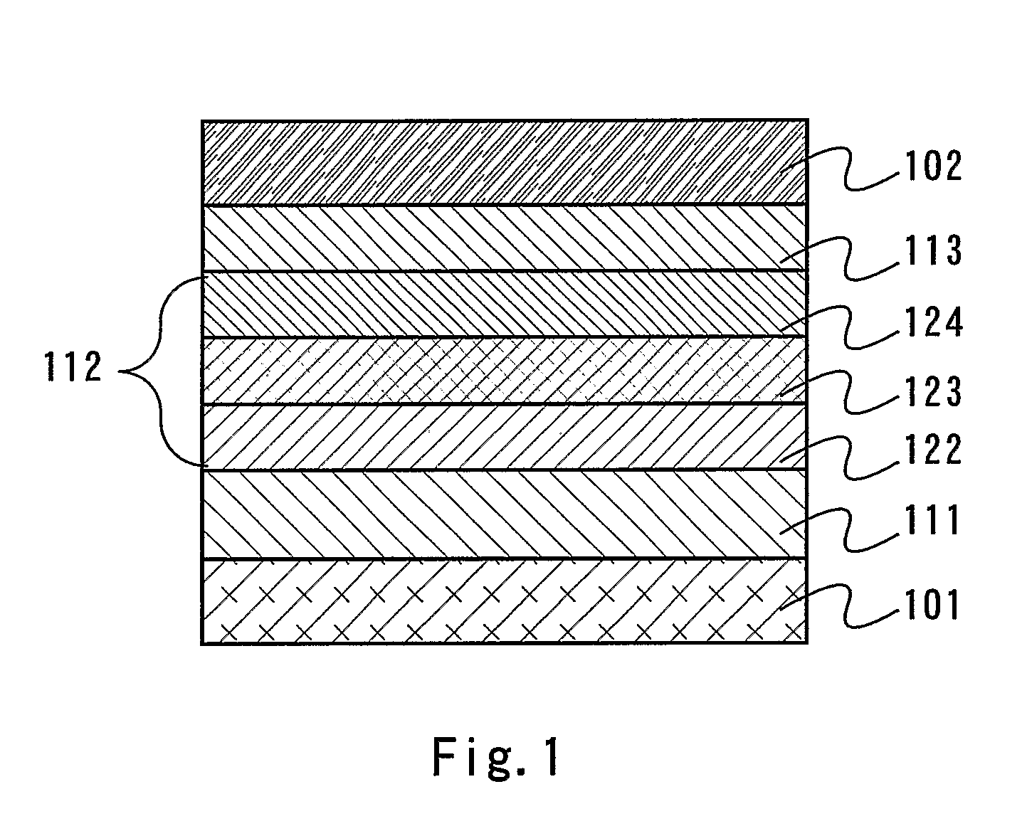
[0055]In the present embodiment, an example of a light-emitting element using a layer including an inorganic compound and an organic compound that has a glass-transition temperature of 150° C. or more, preferably 160° C. or more and 300° C. or less, will be described with reference to FIG. 1, where a benzidine derivative is used as the organic compound. It is to be noted that benzidine derivative according to the present invention is a compound having a spiro ring and a triphenylamine skeleton.

[0056]As shown in FIG. 1, the light-emitting element according to the present invention has a first electrode 101 and a second electrode 102 that are opposed to each other, and has a first layer 111, a second layer 112, and a third layer 113 that are stacked in this order from the first electrode 101 side. When a voltage is applied to this light-emitting element so that the potential of the first electrode 101 is higher than the potential of the second electrode 102, a hole is injected from th...

embodiment 2

[0115]An example of a light-emitting element using a layer including a benzidine derivative according to the present invention, which is a compound having a spiro ring and a triphenylamine skeleton, and an inorganic compound will be described with reference to FIG. 18.

[0116]As shown in FIG. 18, the light-emitting element according to the present invention has a first electrode 101 and a second electrode 102 that are opposed to each other, and has a first layer 111, a second layer 112, and a third layer 113 that are stacked in this order from the first electrode 101 side. When a voltage is applied to this light-emitting element so that the potential of the first electrode 101 is higher than the potential of the second electrode 102, a hole is injected from the first layer 111 into the second layer 112, and an electron is injected from the third layer 113 into the second layer 112. The hole and the electron are recombined to excite a luminescent material. Then, luminescence is produce...

embodiment 3

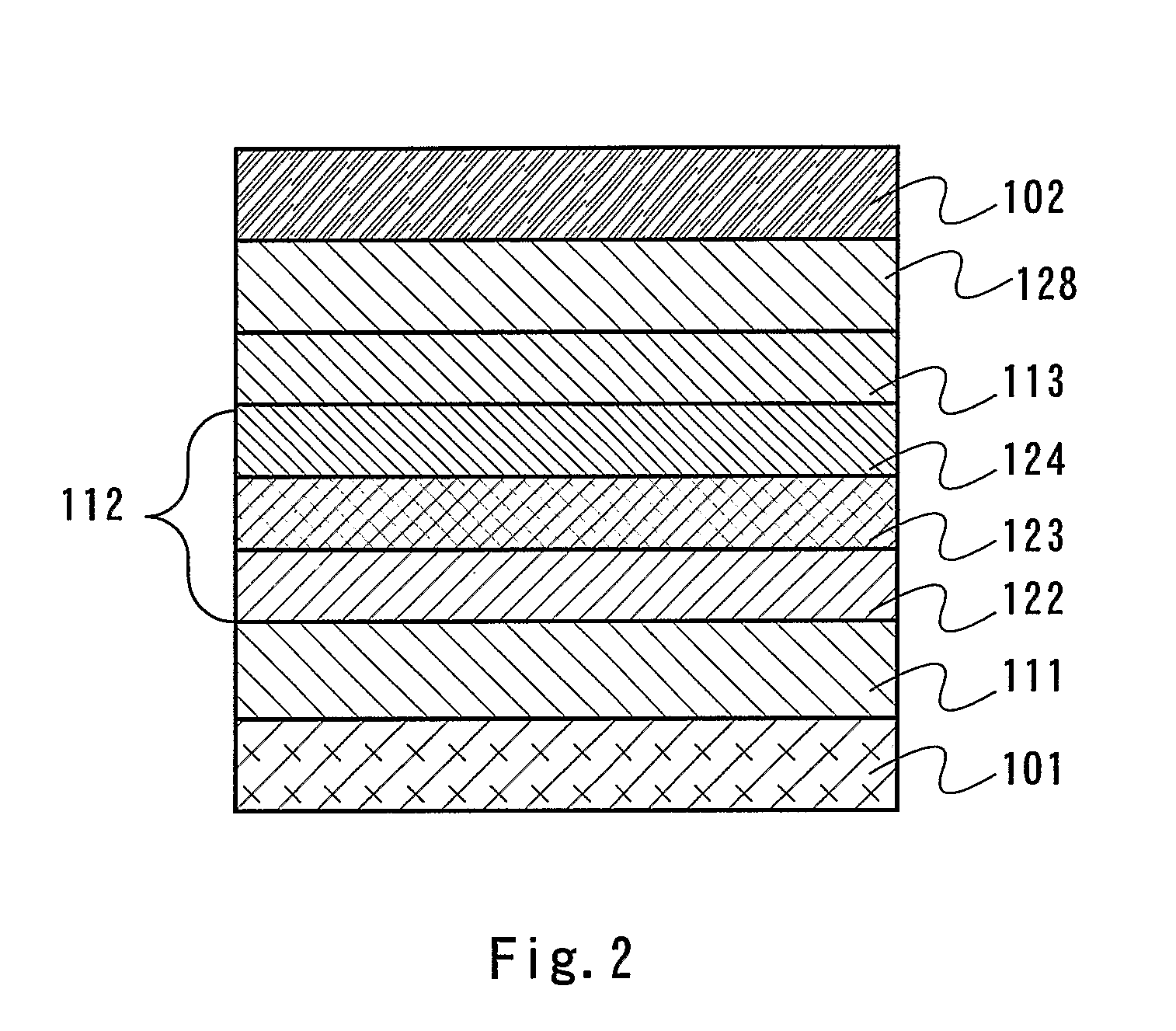
[0173]In the present embodiment, the structure of a light-emitting element that is different from the embodiments-described above will be described.

[0174]As shown in FIG. 2, the light-emitting element shown in the present embodiment has a first electrode 101 and a second electrode 102 that are opposed to each other, and has a first layer 111, a second layer 112, a third layer 113, and a fourth layer 128 that are stacked in this order from the first electrode 101 side, where it is a feature that the fourth layer 128 is provided. The fourth layer 128 can be formed by using the same material as the first layer 111, and the other structure is the same as the embodiment described above. Therefore, description of the structure other than the fourth layer 128 is omitted.

[0175]When the fourth layer 128 is provided in this way, damage during forming the second electrode 102 can be further reduced.

[0176]Further, a layer in which an organic compound and an inorganic compound are mixed is prefe...


PUM

PropertyMeasurementUnit
glass-transition temperatureaaaaaaaaaa

Abstract

The present invention provides a light-emitting element that includes a pair of electrodes, and an organic compound that has a glass-transition temperature of 150° C. or more, preferably 160° C. or more and 300° C. or less, and a metal oxide that are provided between the pair of electrodes, or includes a pair of electrodes, and a compound having a spiro ring and a triphenylamine skeleton and a metal oxide that are provided between the pair of electrodes. It is a feature that the compound has a spiro ring and a triphenylamine skeleton is a benzidine derivative represented by a general formula (1) In the formula, R1 is hydrogen or an alkyl group having 1 to 4 carbon atoms.

Description

TECHNICAL FIELD[0001]The present invention relates to the structure of a light-emitting element including an organic compound and an inorganic compound, and further relates to a light-emitting device that has the light-emitting element.BACKGROUND ART[0002]Many of light-emitting elements that are used for displays have a structure in which a layer including a luminescent material is sandwiched between a pair of electrodes, and luminescence is produced when an exciton formed by recombining an electron injected from one of the electrodes and a hole injected from the other electrode returns to the ground state.[0003]Regarding these light-emitting elements, studies for improving a luminous efficiency and stability and preventing increase in driving voltage have been conducted.[0004]For example, Patent Document 1 discloses a highly durable organic thin-film light-emitting element that is able to keep light-emitting performance. According to Patent Document 1, it is disclosed that a lower ...

Claims


Application Information

Patent Timeline
Patent Type & Authority Applications(United States)
IPC IPC(8): H01J1/62B32B9/00
CPCC07C211/61C07C2103/97C09K11/06C09K2211/1007C09K2211/1011H05B33/14H01L51/0058H01L51/006H01L51/5036H01L51/5052C09K2211/1014Y10S428/917C07C2603/97H10K85/626H10K85/633H10K50/125H10K50/155H10K50/165
Inventor SAKATA, JUNICHIROIKEDA, HISAOKAWAKAMI, SACHIKO
Owner SEMICON ENERGY LAB CO LTD
Why Eureka
Try Eureka