Method of integrating triple gate oxide thickness

a technology of oxide thickness and triple gate, which is applied in the manufacturing of semiconductor/solid-state devices, basic electric elements, electric devices, etc., can solve the problems of reducing the extent of divot formation, and reducing the subthreshold leakage particularly in the low voltage area

Active Publication Date: 2008-05-29
TAIWAN SEMICON MFG CO LTD
View PDF4 Cites 16 Cited by
  • Summary
  • Abstract
  • Description
  • Claims
  • Application Information

AI Technical Summary

Benefits of technology

[0008]In the present invention, the extent of divot formation is advantageously reduced without introducing excessive complexity in ...

Problems solved by technology

However, the oxide removal processes have a detrimental impact on the shallow trench iso...

Method used


Image

  • Method of integrating triple gate oxide thickness
  • Method of integrating triple gate oxide thickness
  • Method of integrating triple gate oxide thickness

Examples


Embodiment Construction

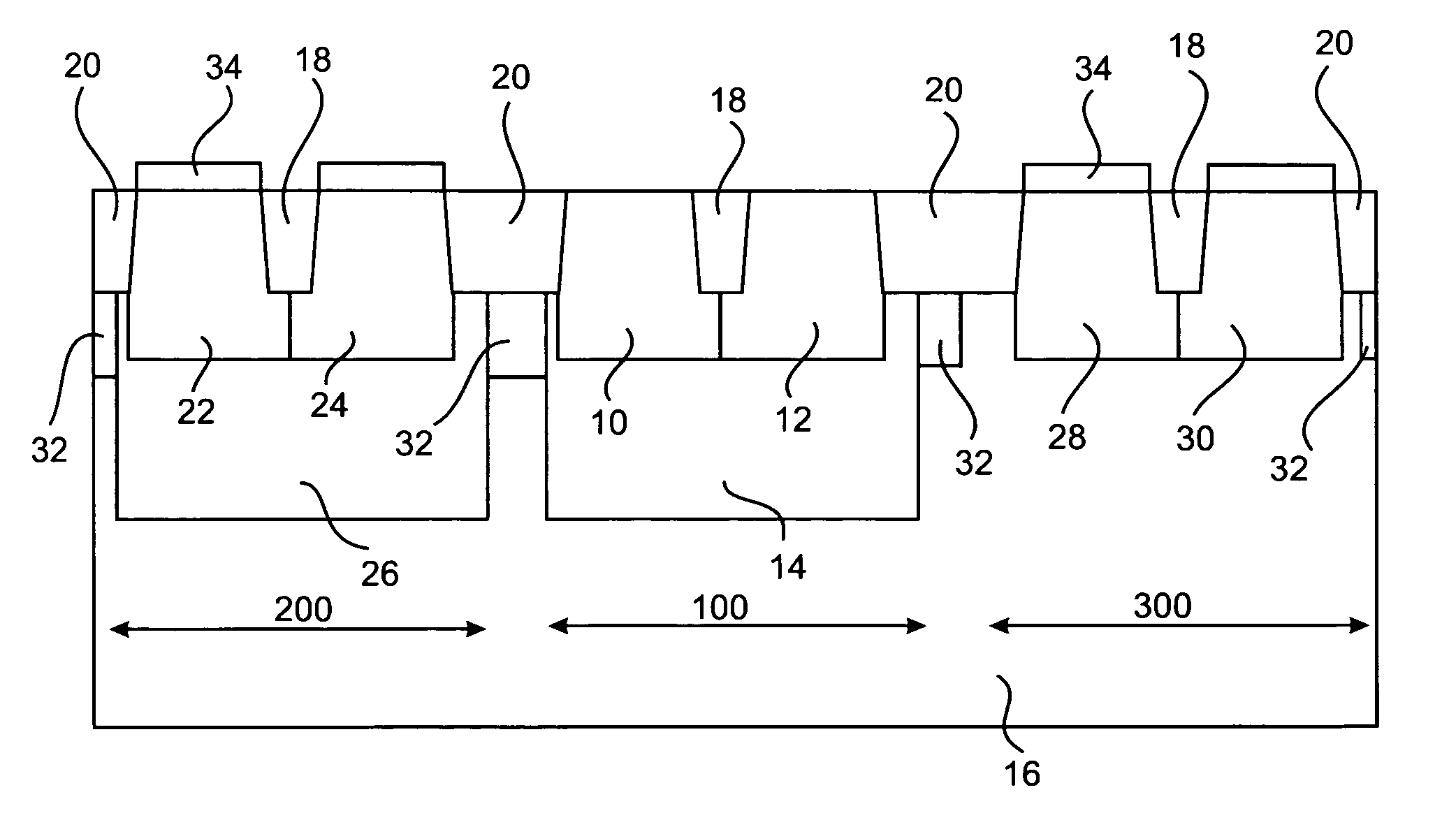
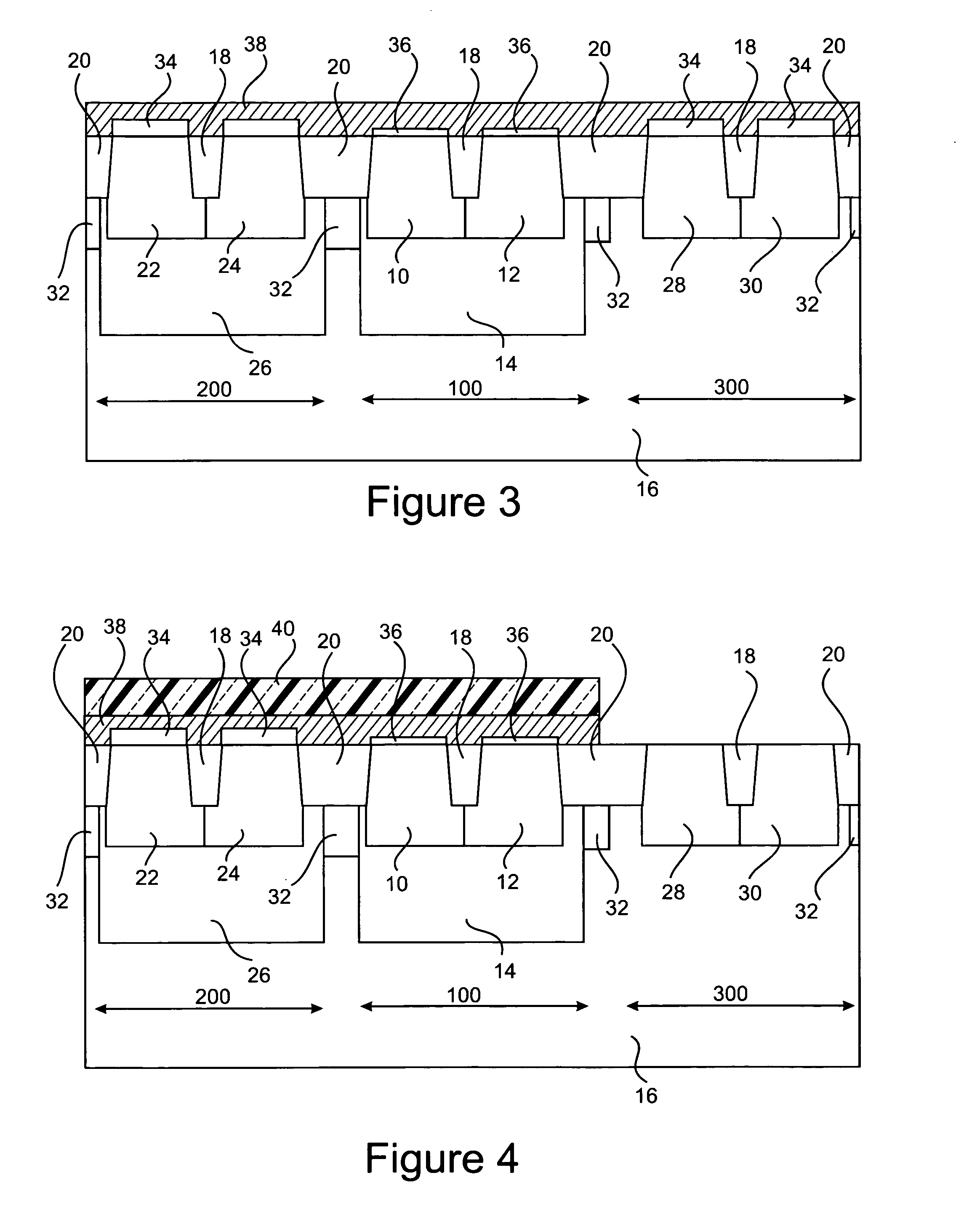
[0012]Preferred embodiments of the invention are described with the aid of FIGS. 2-7 which are various cross-sections of a TGO chip at an intermediate stage of manufacture. In TGO structures there are semiconductor regions of the first kind, for example a low voltage region over which devices with thin gate oxide are formed, semiconductor regions of the second kind, for example an intermediate voltage region over which devices with gate oxides of intermediate thickness are formed and semiconductor regions of the third kind for example, a high voltage region over which devices with thick gate oxide are formed. Correspondingly, there is a low threshold voltage for MOSFET in semiconductor regions of the first kind, an intermediate threshold voltage for MOSFET in semiconductor regions of the second kind and a high threshold voltage for MOSFET in semiconductor regions of the third kind.

[0013]With reference to FIGS. 2-7, in the semiconductor regions of the first kind 100, that is regions ...


PUM


Abstract

A method for forming TGO structures includes providing a substrate containing regions of first, second and third kinds in which devices with respective first, second and third gate oxide layers of different thicknesses are to be formed. The second gate oxide layer is formed over the substrate and then removed from regions of the first kind where the first gate oxide layer is subsequently grown. A first conductive layer is deposited over the substrate. The first conductive layer and second gate oxide layer are subsequently removed from regions of the third kind. The third gate oxide layer followed by deposition of a second conductive layer is formed over the substrate and then removed except from over regions of the third kind.

Description

FIELD OF THE INVENTION[0001]The present invention relates generally to method of manufacturing integrated circuits and in particular to methods of manufacturing field effect transistors (FET) of different gate oxide thicknesses on the same chip.BACKGROUND OF THE INVENTION[0002]The miniaturization of electronic components has made it increasingly common to integrate devices with diverse characteristics on a single integrated circuit (IC) giving rise to what is known as a system on chip (SOC) technology. The various types of devices located on a system on chip IC typically have different operating voltages thus requiring multiple gate oxide layers of different thickness to be formed. For example, a chip may have low, medium and high voltage device regions with the gate oxide associated with the field effect transistors (FET) in the high voltage region being the thickest and the gate oxide associated with the FETs in the low voltage device region being the thinnest. Chips having FETs f...

Claims


Application Information

Patent Timeline
IPC IPC(8): H01L21/77
CPCH01L21/76224H01L21/823462H01L21/823878H01L21/823857H01L21/823481
Inventor VERMA, PURAKH RAJCHU, SANFORDCHUA, HWEE NGOH
Owner TAIWAN SEMICON MFG CO LTD
Why Eureka
Try Eureka