Techniques for low-temperature ion implantation

Active Publication Date: 2008-05-29
VARIAN SEMICON EQUIP ASSOC INC
View PDF11 Cites 46 Cited by
  • Summary
  • Abstract
  • Description
  • Claims
  • Application Information

AI Technical Summary

Benefits of technology

[0012]Techniques for low-temperature ion implantation are disclosed. In one particular exemplary embodiment, the techniques may be realized as an apparatus for low-temperature ion implantation. The apparatus may comprise a wafer support mechanism to hold a wafer during ion implantation and to facilitate movement of the wafer in at least one dimension. The apparatus may also

Problems solved by technology

These interstitials may lead to transient enhanced diffusion (TED) of ion-implanted dopants, causing a resultant dopant profile (e.g., P-N or N-P junction) to deepen and/or lose a desired abruptness.
As a result, a thinner amorphous layer can adversely increase short channel effects in electronic devices.
The interstitials beyond the amorphous-crystalline interface not removed during the activation anneal may combine to form complex end-of-range damage.
This damage can lead to junction leakage and yield loss mechanisms.
The damage may evolve during later thermal processes by emitting interstitials which can lead to further dopant diffusion and dopant deactivation.
Since amorphization of the silicon occurs

Method used


Image

  • Techniques for low-temperature ion implantation
  • Techniques for low-temperature ion implantation
  • Techniques for low-temperature ion implantation

Examples


Embodiment Construction

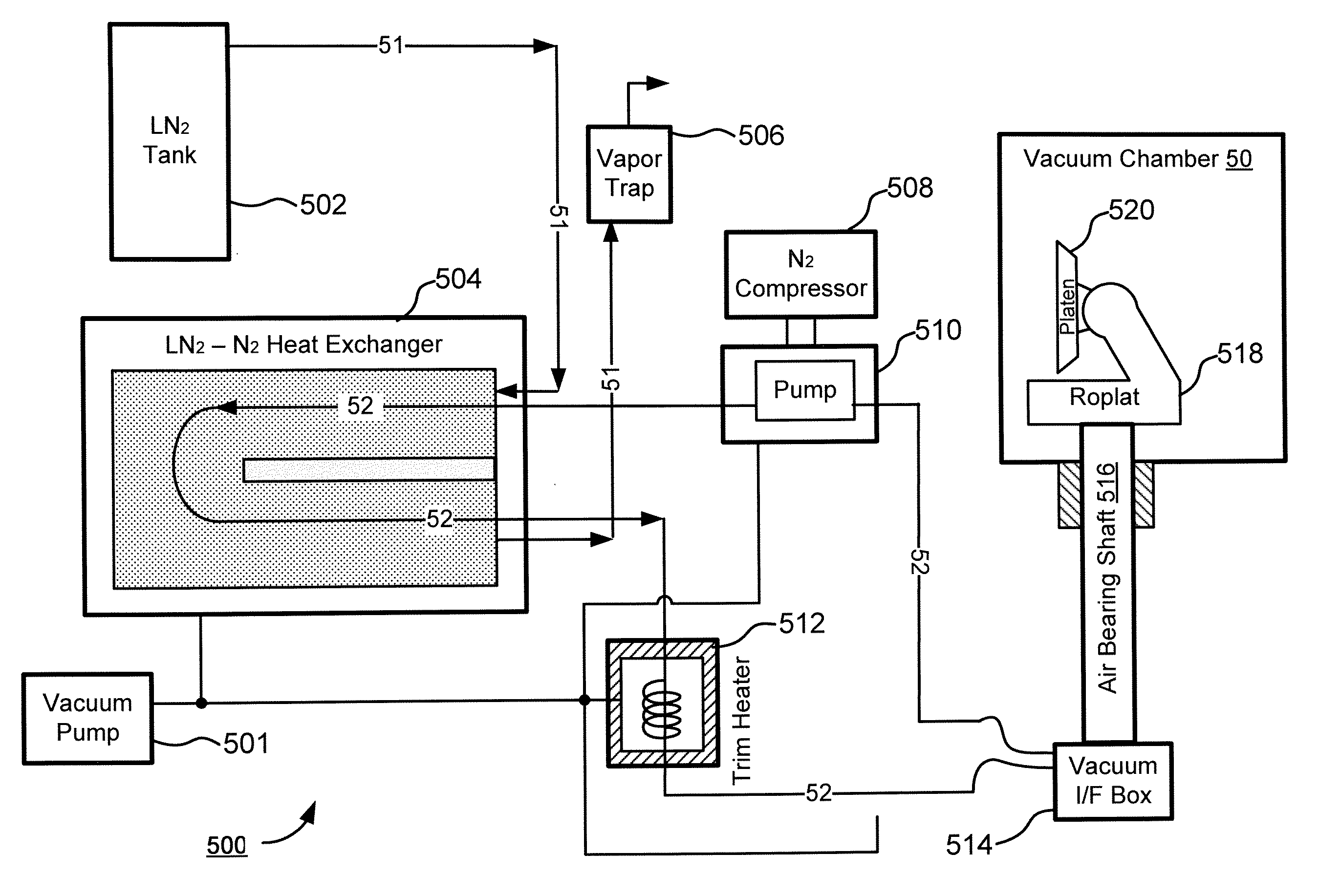
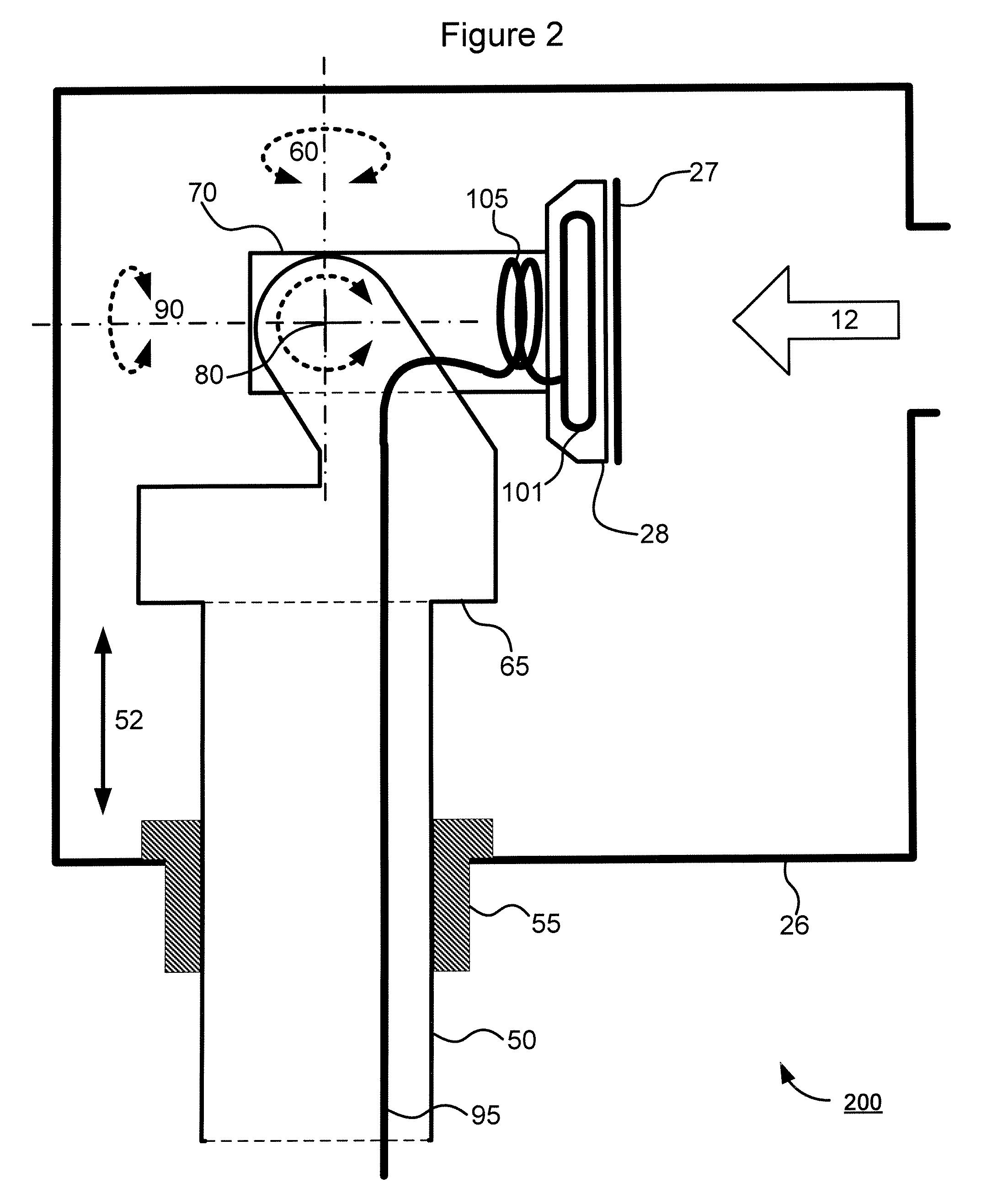
[0023]Embodiments of the present disclosure facilitate direct wafer cooling during low-temperature ion implantation with an improved design of a wafer support and cooling system. In an ion implanter, rigid coolant pipes may be interconnected and coupled to a platen via one or more rotary bearings, wherein the rigid coolant pipes accommodate coolant circulation at a relatively high pressure and the rotary bearings accommodate platen motions. The rigid coolant pipes may be insulated with a vacuum casing to prevent heat loss and condensation. A gaseous coolant may be preferable since a minor leak will not contaminate the ion implanter. More precise control of wafer temperature may be achieved by incorporating a heating element into the cooling system.

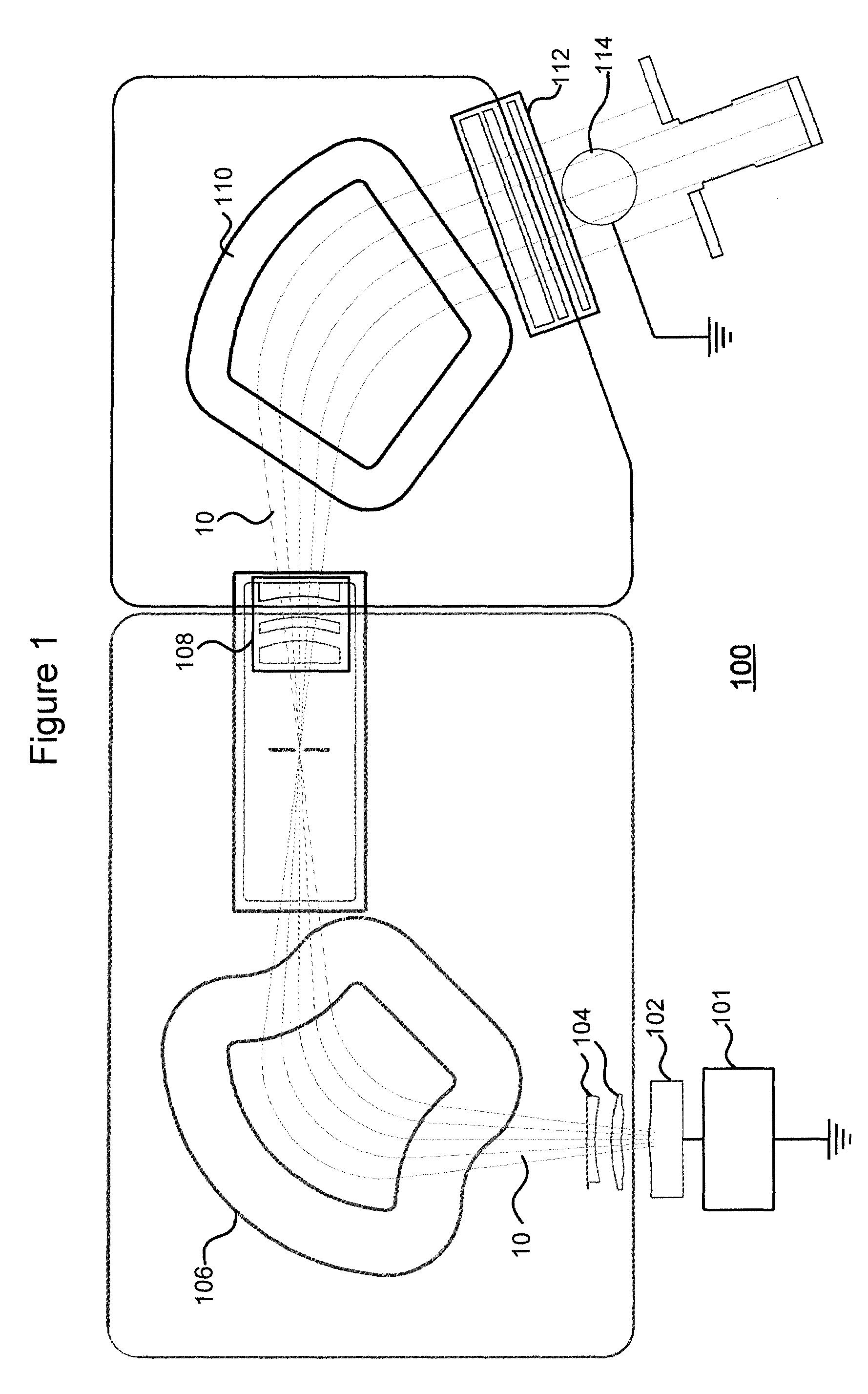
[0024]The techniques disclosed herein are not limited to beam-line ion implanters, but are also applicable to other types of ion implanters such as those used for plasma doping (PLAD) or plasma immersion ion implantation (PIII).

[0025]FIG. ...


PUM

PropertyMeasurementUnit
Temperatureaaaaaaaaaa
Electric potential / voltageaaaaaaaaaa
Dimensionaaaaaaaaaa

Abstract

Techniques for low-temperature ion implantation are disclosed. In one particular exemplary embodiment, the techniques may be realized as an apparatus for low-temperature ion implantation. The apparatus may comprise a wafer support mechanism to hold a wafer during ion implantation and to facilitate movement of the wafer in at least one dimension. The apparatus may also comprise a cooling mechanism coupled to the wafer support mechanism. The cooling mechanism may comprise a refrigeration unit, a closed loop of rigid pipes to circulate at least one coolant from the refrigeration unit to the wafer support mechanism, and one or more rotary bearings to couple the rigid pipes to accommodate the movement of the wafer in the at least one dimension.

Description

CROSS-REFERENCE TO RELATED APPLICATIONS[0001]This patent application claims priority to U.S. Provisional Patent Application No. 60 / 861,160, filed Nov. 27, 2006, which is hereby incorporated by reference herein in its entirety.[0002]This patent application is related to U.S. patent application Ser. No. 11 / 504,367, filed Aug. 15, 2006, which is hereby incorporated by reference herein in its entirety.FIELD OF THE DISCLOSURE[0003]The present disclosure relates generally to semiconductor manufacturing and, more particularly, to techniques for low-temperature ion implantation.BACKGROUND OF THE DISCLOSURE[0004]With continued miniaturization of semiconductor devices, there has been an increased demand for ultra-shallow junctions. For example, tremendous effort has been devoted to creating better activated, shallower, and more abrupt source-drain extension junctions to meet the needs of modern complementary metal-oxide-semiconductor (CMOS) devices.[0005]To create an abrupt, ultra-shallow jun...

Claims


Application Information

Patent Timeline
IPC IPC(8): H01L21/425C23C14/00
CPCH01J37/3171H01L21/67005H01J2237/2001H01J37/30H01L21/265
Inventor ENGLAND, JONATHAN GERALDMUKA, RICHARD STEPHENLISCHER, D. JEFFREY
Owner VARIAN SEMICON EQUIP ASSOC INC
Why Eureka
Try Eureka