Apparatus and method for introducing particles using a radio frequency quadrupole linear accelerator for semiconductor materials

a technology of quadrupole linear accelerator and apparatus, which is applied in the direction of accelerators, electric discharge tubes, basic electric elements, etc., can solve the problems of low efficiency of solar cells, and many limitations of solar cells, and achieve high quality, cost-effective, and highly efficient photovoltaic cells

Inactive Publication Date: 2008-06-05
SILICON GENERAL CORPORATION
View PDF74 Cites 106 Cited by
  • Summary
  • Abstract
  • Description
  • Claims
  • Application Information

AI Technical Summary

Benefits of technology

[0012]Numerous benefits are achieved over pre-existing techniques using embodiments of the present invention. In particular, embodiments of the present invention use an apparatus and method including using a cost effective linear accelerator system and a beam expander to provide a particle beam for high-energy implant process for thick layer transfer techniques. Such linear accelerator system may include, but is not limited to, a drift tube technique, a Radio Frequency Quadrupole, commonly called RFQ, Radio Frequency Interdigited (commonly known as RFI), or other linear acceleration methods, or combinations of these, and other suitable techniques. In a specific embodiment, the apparatus includes a beam expander that provides a beam with desired power flux sufficiently lower than a minimum flux to causing the excessive damage to the material to be implanted but high enough to uniformly apply on workpiece in square meter size or like with an efficient process. In a preferred embodiment, the linear accelerator system provides an implantation process that forms a thickness of transferable material defined by a cleave plane in a donor substrate. The thickness of transferable material may be further processed to provide a high quality semiconductor material for application such as photovoltaic devices, 3D MEMS or integrated circuits, IC packaging, semiconductor devices, any combination of these, and others. In a preferred embodiment, the present method provides for single crystal silicon thick film for highly efficient photovoltaic cells among others. An alternative preferred embodiment according to the present invention may provide for a seed layer that can further provide for layering of a hetero-structure epitaxial process. The hetero-structure epitaxial process can be used to form thin multi-junction photovoltaic cells, among others. Merely as an example, GaAs and GaInP layers may be deposited heteroepitaxially onto a germanium seed layer, which is a transferred layer formed using an implant process according to an embodiment of the present invention. Depending upon the embodiment, one or more of these benefits may be achieved.

Problems solved by technology

Unfortunately, such petroleum sources have become depleted and have lead to other problems.
Although effective, these solar cells still have many limitations.
These materials are often difficult to manufacture.
Although these plates may be formed effectively, they do not possess optimum properties for highly effective solar cells.
Such single crystal silicon is, however, expensive and is also difficult to use for solar applications in an efficient and cost effective manner.
Generally, thin-film solar cells are less expensive but less efficient than the more expensive bulk silicon cells made from single-crystal silicon substrates.
Although successful, there are still many limitations with conventional techniques for forming solar cells or other films of materials.

Method used


Image

  • Apparatus and method for introducing particles using a radio frequency quadrupole linear accelerator for semiconductor materials
  • Apparatus and method for introducing particles using a radio frequency quadrupole linear accelerator for semiconductor materials
  • Apparatus and method for introducing particles using a radio frequency quadrupole linear accelerator for semiconductor materials

Examples


Embodiment Construction

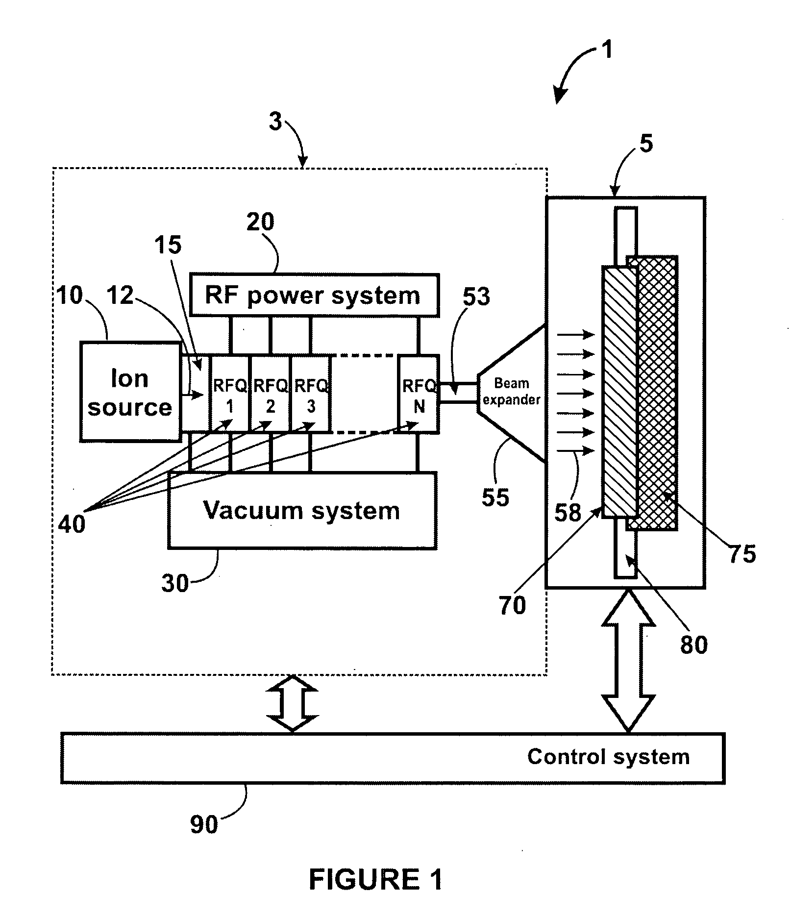
[0027]The present invention relates generally to techniques including an apparatus and a method of introducing charged particles for semiconductor material processing. More particularly, the present apparatus and method provide a system using a linear accelerator, for example a radio frequency quadrupole linear accelerator, to obtain a beam of particles with MeV energy level for manufacturing one or more detachable semiconductor film that is capable of free-standing for device applications including photovoltaic cells. But it will be recognized that the invention has a wider range of applicability; it can also be applied to other types of applications such as for three-dimensional packaging of integrated semiconductor devices, photonic or optoelectronic devices, piezoelectronic devices, flat panel displays, microelectromechanical systems (“MEMS”), nano-technology structures, sensors, actuators, integrated circuits, biological and biomedical devices, and the like.

[0028]For purposes o...


PUM


Abstract

A system for forming one or more detachable semiconductor films capable of being free-standing. The apparatus includes an ion source to generate a plurality of collimated charged particles at a first energy level. The system includes a linear accelerator having a plurality of modular radio frequency quadrupole (RFQ) elements numbered from 1 through N successively coupled to each other, where N is an integer greater than 1. The linear accelerator controls and accelerates the plurality of collimated charged particles at the first energy level into a beam of charge particles having a second energy level. RFQ element numbered 1 is operably coupled to the ion source. The system includes an exit aperture coupled to RFQ element numbered N of the RFQ linear accelerator. In a specific embodiment, the system includes a beam expander coupled to the exit aperture, the beam expander being configured to process the beam of charged particles at the second energy level into an expanded beam of charged particles. The system includes a process chamber coupled to the beam expander and a workpiece provided within the process chamber to be implanted

Description

CROSS-REFERENCE TO RELATED APPLICATION[0001]The instant nonprovisional patent application claims priority to U.S. Provisional Patent Application No. 60 / 864,966, filed Nov. 8, 2006 and incorporated by reference in its entirety herein for all purposes.BACKGROUND OF THE INVENTION[0002]Embodiments in accordance with the present invention relate generally to techniques including an apparatus and a method of introducing charged particles for semiconductor material processing. More particularly, embodiments of the present apparatus and method provide a system using a linear accelerator (Linac), such as a radio frequency quadrupole linear accelerator, to obtain a beam of particles with MeV energy level for manufacturing one or more detachable semiconductor film that is capable of free-standing for device applications including photovoltaic cells. But it will be recognized that the invention has a wider range of applicability; it can also be applied to other types of applications such as for...

Claims


Application Information

Patent Timeline
Patent Type & Authority Applications(United States)
IPC IPC(8): G21K5/10H05H9/00
CPCH01J37/04H01J37/3171H01J2237/04737H05H9/00H05H7/04H05H7/10H01L21/26506H01L21/26593H01L21/2658H05H7/00H01L21/425G21K5/10
Inventor HENLEY, FRANCOIS J.LAMM, ALBERTADIBI, BABAK
Owner SILICON GENERAL CORPORATION
Why Eureka
Try Eureka