Monolithic electronic component

a technology of electronic components and monolithic materials, applied in the direction of fixed capacitor details, semiconductor/solid-state device details, instruments, etc., can solve the problems of difficult to form a plating film with a uniform thickness, difficult to perform electroplating, and inability to easily flow electric current during electroplating, etc., to achieve the effect of stabilizing resistance and conductive resin films

Active Publication Date: 2008-06-05
MURATA MFG CO LTD
View PDF1 Cites 23 Cited by
  • Summary
  • Abstract
  • Description
  • Claims
  • Application Information

AI Technical Summary

Benefits of technology

[0020]Therefore, when in the resistive terminal electrode aplating film is formed on the conductive resin film preferably via electroplating, the thickness of the plating film can be made uniform. Thus, moisture resistance of the monolithic electronic component can be ensured, and changes in resistance due to heat during, for example, a mounting step can be suppressed. When the plating film has a bi-layer structure including a layer of a metal, such as Ni for example, which is not meltable at the solder melting temperature, and a layer formed thereon and made of a metal, such as Sn for example, having good solder wettability, the sealing property of the resistive terminal electrode against moisture can be ensured and heat resistance during a soldering step can be ensured. Furthermore, a good soldering characteristic can be imparted.
[0032]In the case where the monolithic electronic component according to a preferred embodiment of the present invention defines a CR composite component, when the CR composite component is used so as to be provided between apower supply line and a ground, the capacity component of the CR composite component suppresses changes in voltage and the resistance component suppresses resonance. Thus, the power supply voltage can be stabilized.

Problems solved by technology

However, whenperformingelectroplating on the resistor film as disclosed in Japanese Unexamined Patent Application Publication No. 11-283866, if the volume resistivity of the resistor film is high, electric current does not easily flow during electroplating, which makes it difficult to perform the electroplating.
Furthermore, even if a plating film can be formed on the resistor film, it is difficult to form the plating film with a uniform thickness.
As a result, thinner regions of the plating film easily allow entry of moisture and moisture resistance may be degraded.
In addition, since the bonding strength between the resistor film and the plating film is relatively weak when the thickness of the plating film is not uniform, separation of the plating film from the resistor film often occurs when heat is applied during a mounting step or the like, thus leading to changes in resistance.
While the above description relates to monolithic ceramic capacitors, the same problems maybe encountered with other monolithic electronic components having terminal electrodes with resistor films.

Method used


Image

  • Monolithic electronic component
  • Monolithic electronic component
  • Monolithic electronic component

Examples


experimental example 1

[0084]In Experimental Example 1, the adhesion characteristic of a Ni plating film was evaluated by forming on a ceramic element an approximately 30-μm thick resistive foundation film having a specific resistance shown in Table 1 and performing Ni electroplating via barrel plating at a current Dk value of about 0.20 A / dm2 for approximately 60 minutes. The plating film entirely covering the resistive foundation film without exposing any portion of the resistive foundation film was determined to have good plating adhesion. Table 1 shows the number of samples determined to have poor plating adhesion out of a total of 100 samples.

TABLE 1SamplePoor plating adhesionnumberSpecific resistance [Ω· m][number of samples]15 × 10−413 / 100 23 × 10−49 / 10031 × 10−47 / 10047 × 10−50 / 10053 × 10−50 / 100

[0085]As seen in Table 1, poor plating adhesion occurred in Samples 1 to 3 where the specific resistance of the resistive foundation film was about 1×10⁻⁴ Ω·m or greater. Therefore, it is understood that the...

experimental example 2

[0086]In Experimental Example 2, Embodiment Example with conductive resin films and Comparative Example without a conductive resin film were compared in terms of plating film adhesion.

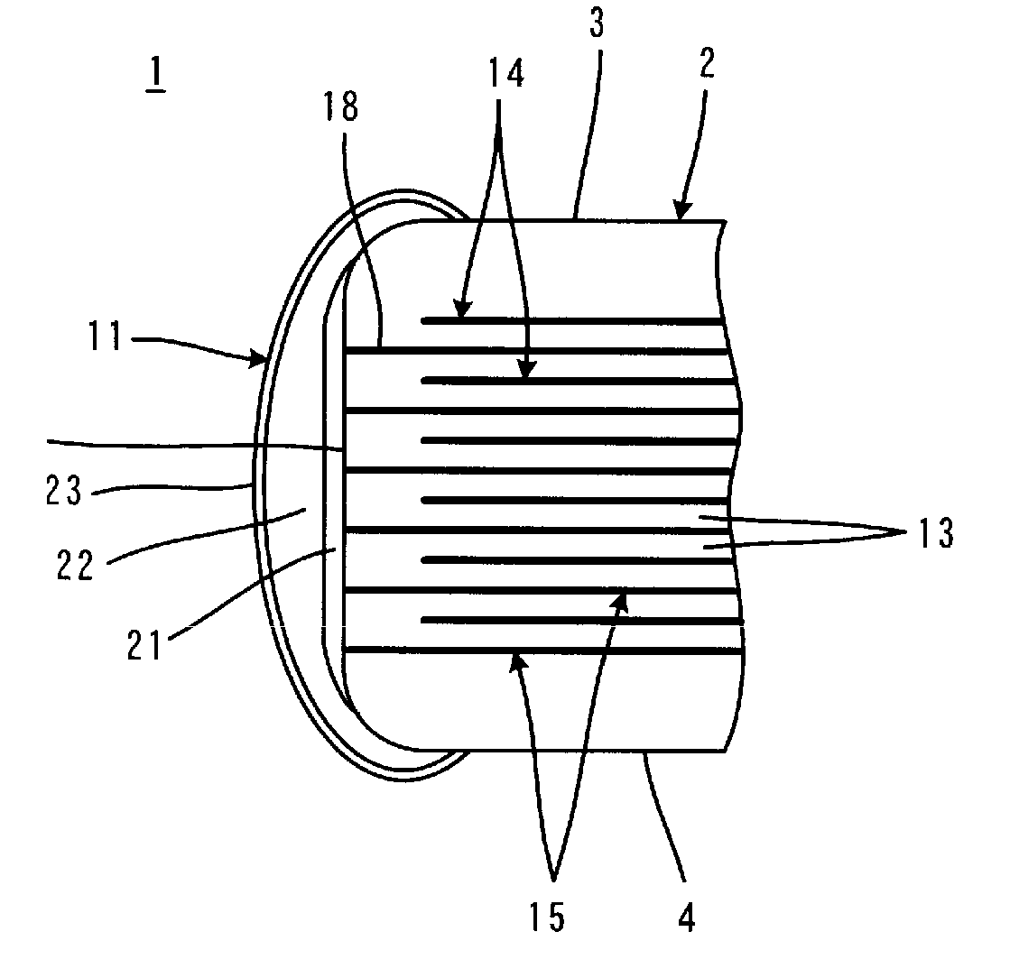
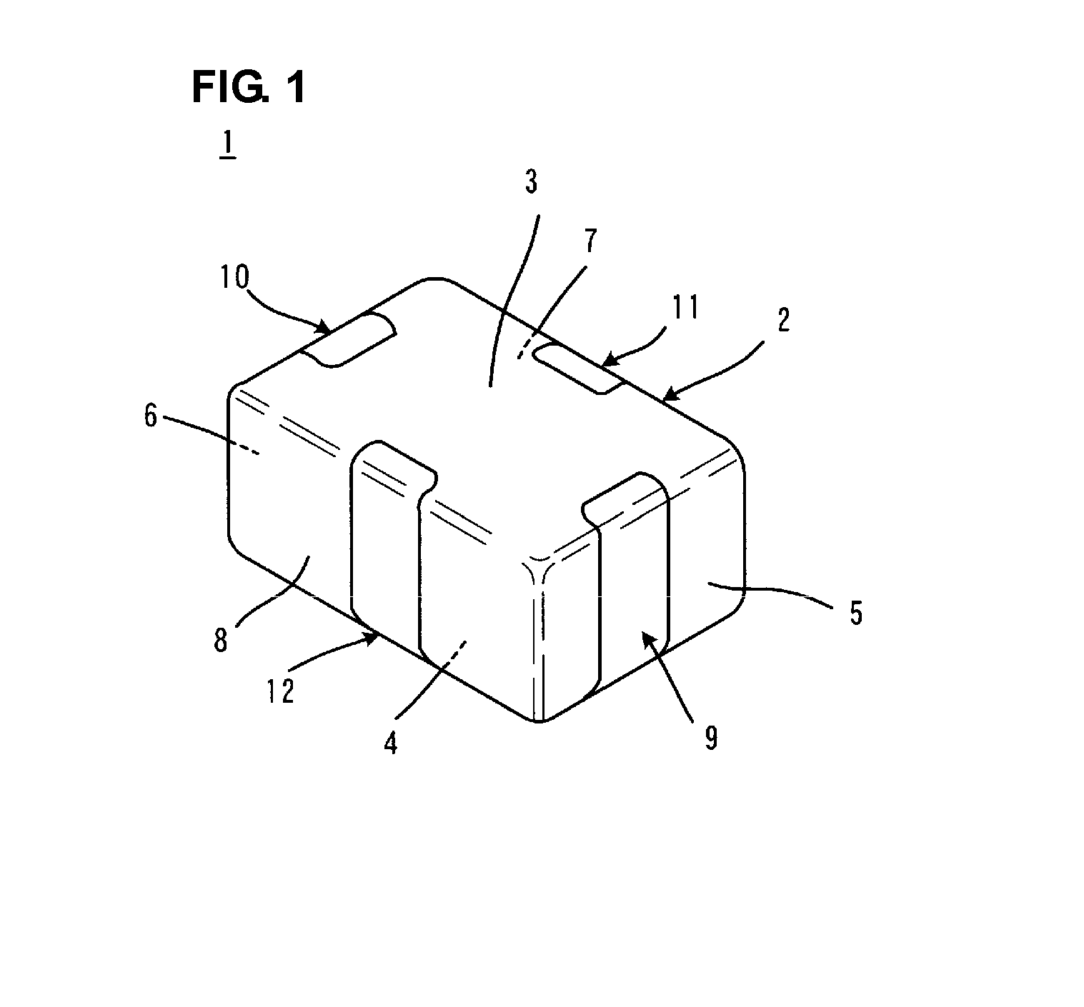
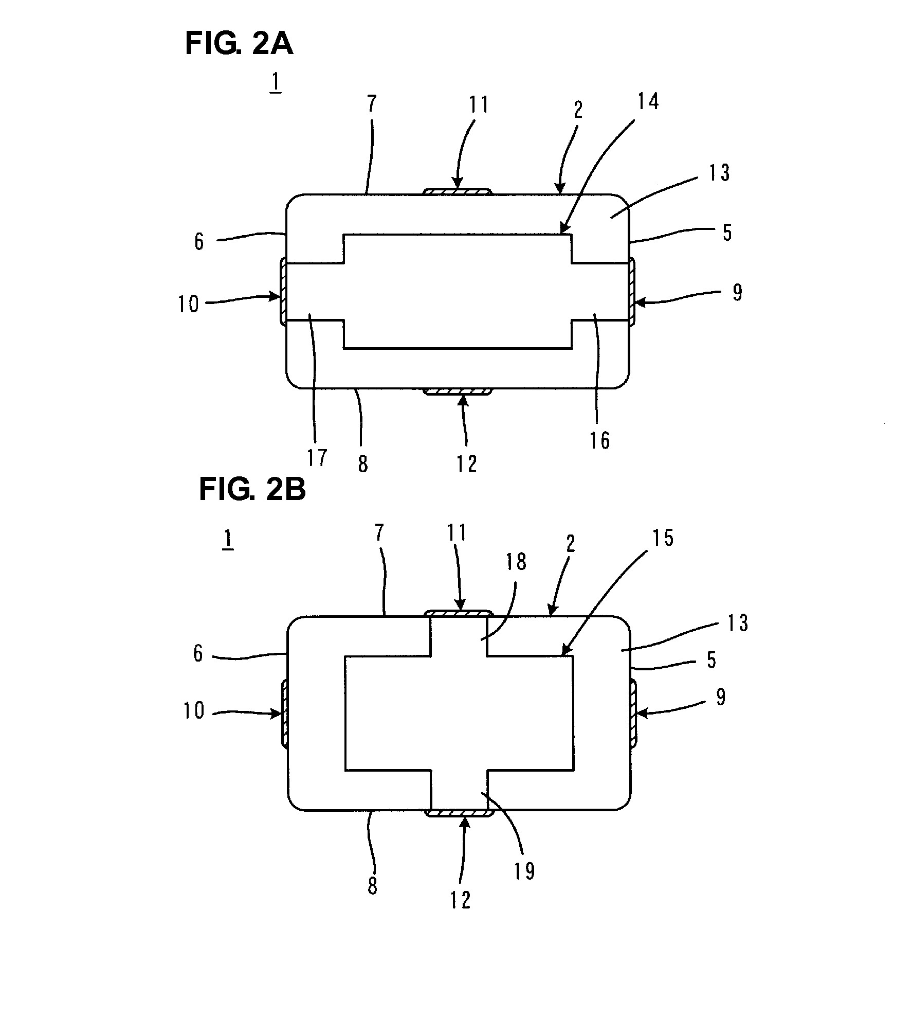
[0087]In both Embodiment Example and Comparative Example, the three-terminal CR composite component 1b having the structure shown in FIG. 6 and FIGS. 7A and 7B was used as samples. The dimensions of the component body 2 were approximately 2.0 mm×1.25 mm×0.85 mm. The first terminal electrodes 9 and 10 served as resistive terminal electrodes, on which a resistor film was formed with a specific resistance of about 5×10⁻³ Ω·m and a thickness of about 30 μm.

[0088]The three-terminal CR composite component 1b used in Embodiment Example had a conductive resin film having a specific resistance of 3×10⁻⁵ Ω·m formed on the resistor film.

[0089]The samples used in Embodiment Example and Comparative Example were subjected to Ni electroplating for approximately 70 minutes via barrel plating at current Dk values of ap...

experimental example 3

[0091]In Experimental Example 3, Embodiment Example with conductive resin films and Comparative Example without a conductive resin film were compared in terms of uniformity of plating film thickness.

[0092]In Experimental Example 3, the same samples as those in Experimental Example 2 were used as samples of Embodiment Example and Comparative Example, and electroplating was conducted under the same conditions as those in Experimental Example 2 except that the current Dk value was set to about 0.28 A / dm2 in Embodiment Example and except that the current Dk value was set to about 0.43 A / dm2 in Comparative Example. Then, a cross-section of the resultant Ni plating film was polished, and the thickness of the Ni plating film was measured with a digital microscope (1000× magnification) . In Comparative Example, where no Ni plating film was formed on some samples, the average thickness and standard deviation of the thickness of the Ni plating film were calculated for 18 samples on which a Ni...


PUM

PropertyMeasurementUnit
self-resonance frequencyaaaaaaaaaa
pressureaaaaaaaaaa
temperatureaaaaaaaaaa

Abstract

In a monolithic electronic component in which a resistive element is incorporated by forming a resistor film on a terminal electrode, a plating film can be formed on the terminal electrode having the resistor film via electroplating in an efficient manner and with a uniform film thickness. In order to form the terminal electrode, the resistor film is disposed directly on the surface of the component body, and a conductive resin film having a relatively low volume resistivity is disposed over the resistor film. The conductive resin film is preferably adapted to have a specific resistance of less than about 1×10⁻⁴ Ω·m, on which a plating film having a uniform film thickness can be formed efficiently via electroplating.

Description

BACKGROUND OF THE INVENTION[0001]1. Field of the Invention[0002]The present invention relates to monolithic electronic components, and more particularly, to the structure of terminal electrodes disposed on the external surfaces of a component body having a monolithic structure so as to be electrically connected to internal electrodes.[0003]2. Description of the Related Art[0004]In general, the noise of an IC power supply line is removed by connecting a bypass capacitor between the power supply line and the ground. When a printed circuit board that is almost entirely covered with a power supply conductor pattern or a grounding conductor pattern is used in order to achieve high-density mounting, resonance often occurs between the power supply and the ground. Since the occurrence of resonance leads to the occurrence of radiation noise, resonance needs to be suppressed.[0005]However, if amonolithic ceramic capacitor, whichtypically has anequivalent series resistance (ESR) as small as se...

Claims


Application Information

Patent Timeline
Patent Type & Authority Applications(United States)
IPC IPC(8): H01L29/00
CPCH01G4/232H01G4/30H01G4/2325H01G4/40H01C7/00H01G4/12H01G4/252
Inventor SAWADA, TAKASHIHADANO, KENJIRO
Owner MURATA MFG CO LTD
Why Eureka
Try Eureka