Memory device and method for performing write operations in such a memory device

a memory device and write operation technology, applied in the direction of information storage, static storage, digital storage, etc., can solve the problems of power consumption, significant power consumption associated with the memory device, and the achievement of low voltage memory device, so as to improve the speed of write operation, reduce the supply voltage, and reduce the supply voltage

Active Publication Date: 2008-06-05
ARM LTD
View PDF2 Cites 25 Cited by
  • Summary
  • Abstract
  • Description
  • Claims
  • Application Information

AI Technical Summary

Benefits of technology

[0013]It has also been found that in many embodiments the additional coupling circuitry can be provided in a manner which has little impact on the overall area of the memory device, and accordingly can have less of a cost impact when compared with the earlier-mentioned prior art technique.
[0015]The additional coupling circuitry provided in memory devices according to embodiments of the present invention can take a variety of forms. In one embodiment, said additional coupling circuitry comprises a booster circuit connected between said first coupling circuitry and said second voltage, at the start of the programming interval the booster circuit connecting said first coupling circuitry to said second voltage, and at said predetermined time said booster circuit being triggered to isolate the first coupling circuitry from the second voltage, charge within the booster circuit causing the at least one bit line to transition beyond said second voltage towards said third voltage. Hence, such a mechanism provides a simple and affective technique for causing the at least one bit line to transition beyond the second voltage towards the third voltage, thereby improving writeability.
[0016]Whilst a separate booster circuit can be provided for each column of memory cells, in one embodiment the booster circuit is shared amongst bit lines associated with multiple columns of memory cells within the memory array. This reduces the impact of the booster circuit on the area of the memory device, thereby reducing the cost of the memory device.
[0020]In one embodiment, a control signal issued to said first coupling circuitry is further routed to a buffer to cause the buffer to generate at said predetermined time the second voltage placed on said additional wire associated with said at least one bit line. In particular, in one embodiment, when the at least one bit line has transitioned to the second voltage, a control signal is issued to the first coupling circuitry to turn that circuitry off, and this signal is used to cause the buffer to transition the associated additional wire to the second voltage. At this time, the capacitance between the relevant bit line and its associated additional wire causes that bit line to transition beyond the second voltage towards the third voltage, thereby improving writeability.

Problems solved by technology

Power consumption is particularly an issue in hand held or mobile devices such as laptops, mobile phones, PDAs, etc, since the power consumption of such a device has a large impact on the battery life.
Therefore, the proportion of power consumption associated with the memory device is significant and will continue to increase as memory capacity increases.
Whilst lowering supply voltage can significantly reduce power consumption, it can cause problems, particularly in respect of the operation of memory devices.
A significant barrier to achieving low voltage memory devices is the increase in process variation that occurs with process scaling.
This causes stability problems within the individual memory cells, and this stability problem is aggravated at lower operating voltages.
In particular, a reduction in the nominal supply voltage is accompanied by a reduction in device noise margins, making components more vulnerable to power supply noise.
This noise consists of AC noise caused by the dynamic AC voltage fluctuation due to the frequency-dependent distributed parasitics inherent in power distribution systems, and DC noise caused by capacitive mismatch.
Hence, the more embedded a particular memory device is within the SoC, the higher the IR drop will be, and hence the greater the noise, thereby further reducing the stability of the cells.
In particular, such noise can cause the state stored in individual memory cells to flip and it is accordingly important to try and avoid this occurring.
However, when such transistors are made larger, it has a negative impact on the writeability of the cell, in that the write operation will typically take longer when larger cells are used.
However, as memory devices become smaller, there is an increase in process variation which causes a stability problem that is aggravated when using low supply voltages.
In seeking to provide resilience to this stability problem, a side effect is that writeability tends to become compromised.
Whilst controlling the supply voltage in such a way improves the write margin, and hence increases write speed, it tends to decrease the data retention stability of the cell.
However, when a write operation is not being performed, the PMOS isolation transistor is turned on, and the PMOS on-resistance gives rise an IR drop associated with that component which thereby gives a lower effective supply voltage at the memory cell, thereby reducing the static noise margin and hence reducing the stability of the cell.
Further, the slightly reduced effective supply voltage is likely to slow down the read operation.
As an additional issue, there is a limit on the number of cells that can share the same PMOS isolation transistor, as decided by the capacitance of the floating line.
In particular, the more cells that the isolation transistor is shared with, the higher the capacitance on the floating line, and the less the performance improvement of the write operation.
As a result, a significant number of such PMOS isolation transistors will be required, and this will have a significant impact on area, and hence the cost, of a device constructed in such a manner.

Method used


Image

  • Memory device and method for performing write operations in such a memory device
  • Memory device and method for performing write operations in such a memory device
  • Memory device and method for performing write operations in such a memory device

Examples


Embodiment Construction

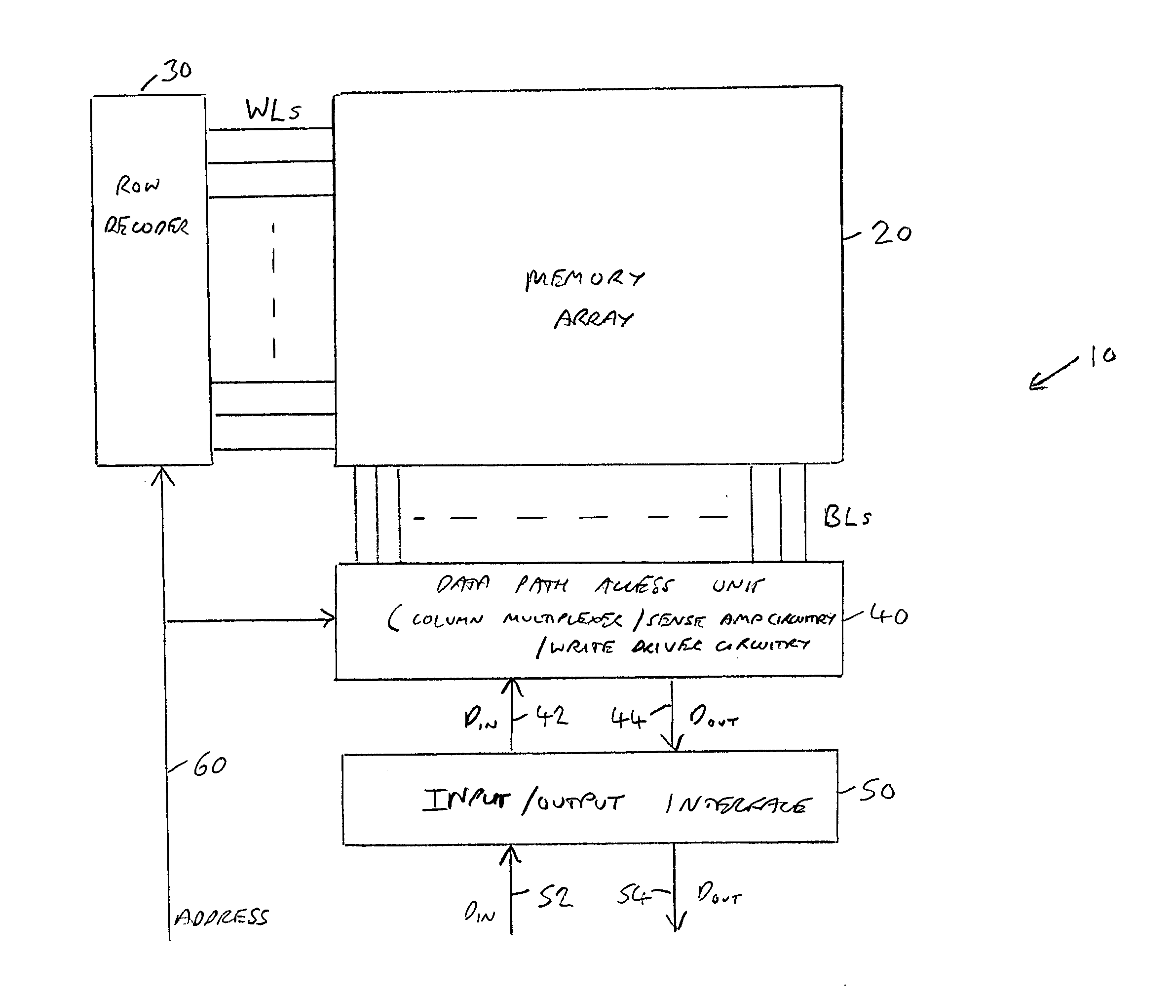
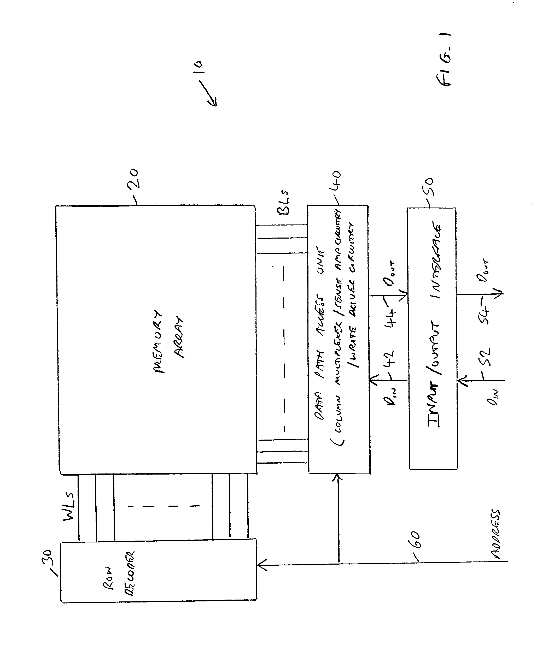
[0034]FIG. 1 is a block diagram of a memory device 10 in accordance with one embodiment of the present invention. The memory device 10 has a memory array 20 consisting of a plurality of memory cells arranged in rows and columns. Each row has a word line (WL) connected thereto, and each column has at least one bit line (BL) connected thereto, the exact number of bit lines connected to each column being depending on embodiment. In one particular embodiment, the memory array consists of SRAM cells, and a pair of bit lines are connected to each column of cells.

[0035]When a memory access request is received, the address specified by the memory access request is routed over path 60 to a row decoder 30 and to a data path access unit 40. The row decoder 30 is arranged to decode the address and dependent thereon drive a control signal over one of the word lines in order to select one of the rows within the memory array 20. Similarly, the data path access unit 40 is arranged dependent on the ...


PUM


Abstract

A memory device and method of performing a write operation in such a memory device are provided. The memory device comprises a memory array having a plurality of memory cells, and a plurality of word lines and a plurality of bit lines via which the plurality of memory cells are accessed. Write driver circuitry is responsive to a write request to write data into at least one memory cell during a programming interval by altering voltage on at least one of the bit lines connected to that at least one memory cell whilst one of the word lines connected to the at least one memory cell is selected, to cause a value indicative of the data to be stored in the at least one memory cell. At a start of the programming interval the at least one bit line is at a first voltage, and the write driver circuitry comprises first coupling circuitry responsive to the write request to couple the at least one bit line to a second voltage to cause the voltage on that at least one bit line to transition towards the second voltage. The first and second voltages represent the operating voltages of the memory cells. Further, additional coupling circuitry is provided which is triggered at a predetermined time during the programming interval to cause the at least one bit line to transition beyond the second voltage towards a third voltage. It has been found that such an approach significantly improves the writeability of memory cells within a memory device arranged to operate at low supply voltages.

Description

BACKGROUND OF THE INVENTION[0001]1. Field of the Invention[0002]The present invention relates to a memory device and method of performing write operations in such a memory device.[0003]2. Description of the Prior Art[0004]It is generally desirable to seek to reduce the power consumption of a data processing apparatus, and such a data processing apparatus often includes a memory device for storing the data used by the data processing apparatus. Power consumption is particularly an issue in hand held or mobile devices such as laptops, mobile phones, PDAs, etc, since the power consumption of such a device has a large impact on the battery life. One approach for seeking to reduce power consumption of a device is to lower the supply voltage used, since lowering the supply voltage reduces the power consumption by a square law. Hence, there are significant benefits in reducing the supply voltage to a device such as a system-on-chip (SoC). Often, SoC devices have large embedded memory devic...

Claims


Application Information

Patent Timeline
Patent Type & Authority Applications(United States)
IPC IPC(8): G11C7/00
CPCG11C11/413
Inventor NAUTIYAL, VIVEK
Owner ARM LTD
Why Eureka
Try Eureka