Producing method of wired circuit board

a production method and wired circuit technology, applied in the direction of conductive pattern formation, non-metallic protective coating application, circuit electrostatic discharge protection, etc., can solve the problems of corrosion and discoloration of the terminal parts, and achieve the effect of efficient removal of static electricity

Inactive Publication Date: 2008-06-12
NITTO DENKO CORP
View PDF9 Cites 10 Cited by
  • Summary
  • Abstract
  • Description
  • Claims
  • Application Information

AI Technical Summary

Benefits of technology

[0026]In the producing method of the wired circuit board, the conductive polymer is polyaniline. Accordingly, the obtained wired circuit board allows more efficient removal of static electricity from the obtained wired circuit board.

Problems solved by technology

This may result in corrosion and discoloration of the terminal portions.

Method used


Image

  • Producing method of wired circuit board
  • Producing method of wired circuit board
  • Producing method of wired circuit board

Examples


example 1

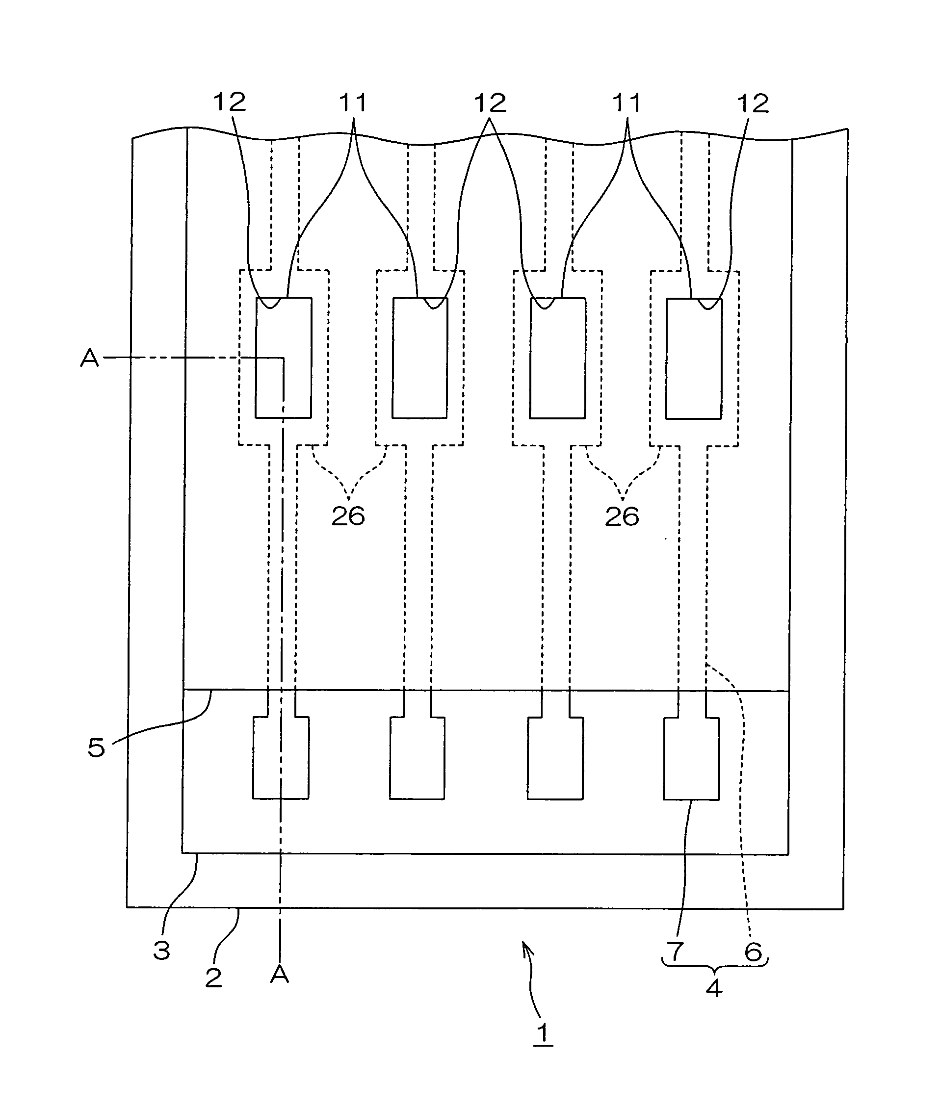
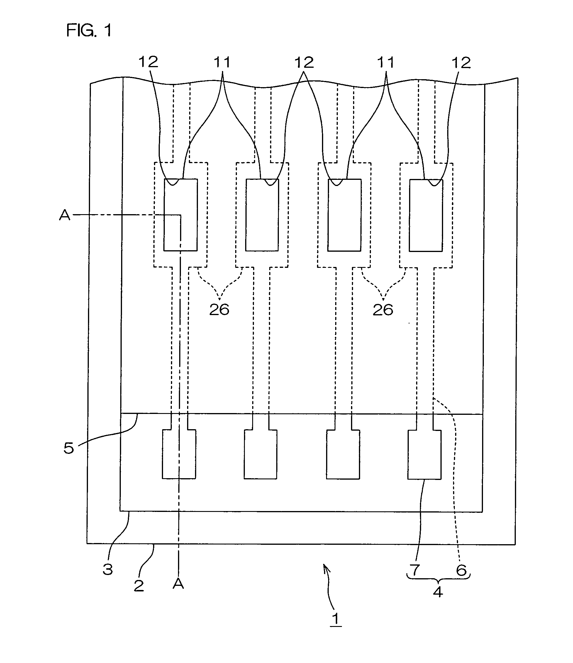
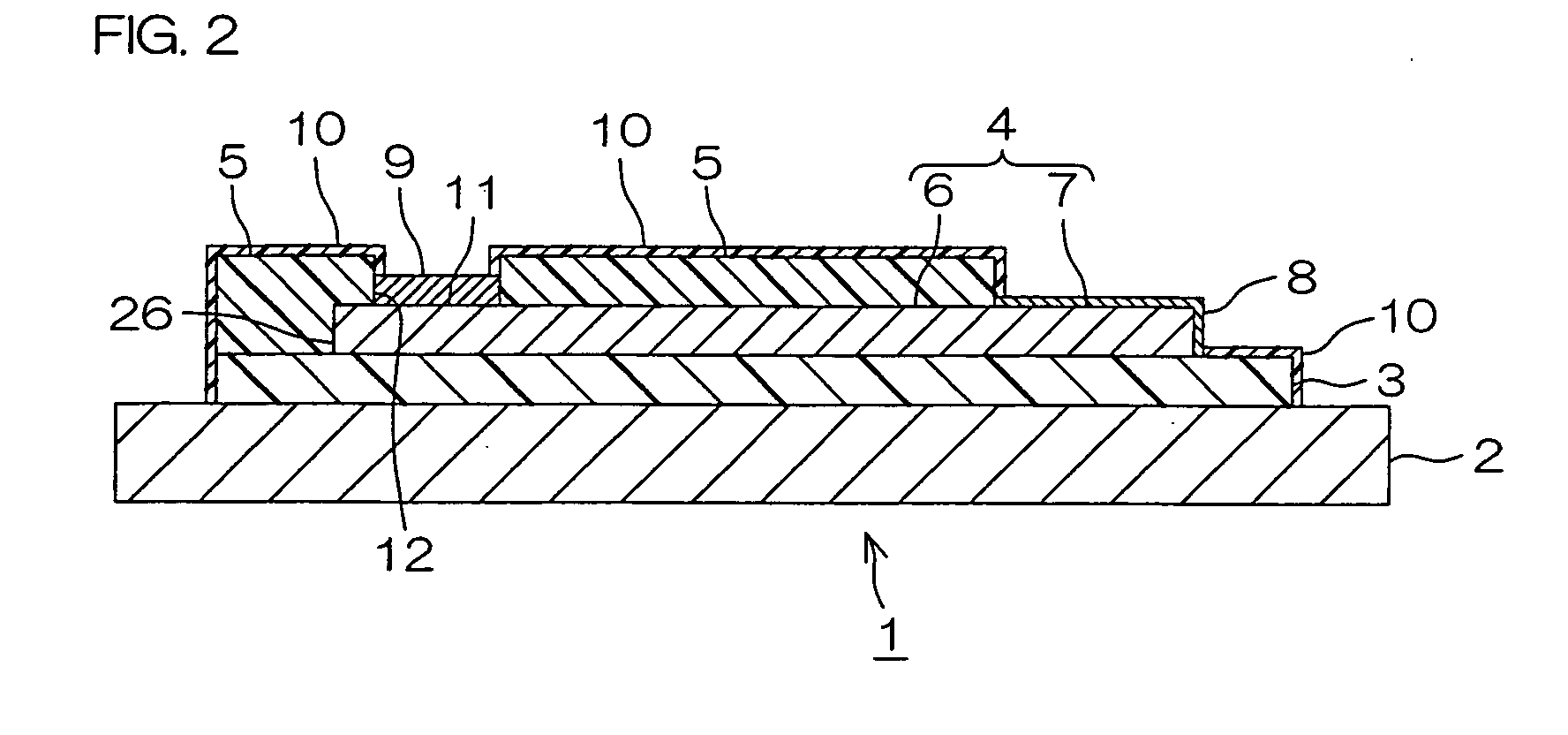
[0168]A metal supporting board made of stainless steel having a thickness of 20 μm was prepared (see FIG. 3(a)).

[0169]Then, a varnish of a photosensitive polyamic acid resin was uniformly coated on the upper surface of the metal supporting board using a spin coater. Then, the coated varnish was heated at 90° C. for 15 minutes to form a base coating. Thereafter, the base coating was exposed to light at 700 mJ / cm2 via a photomask, heated at 190° C. for 10 minutes, and then developed using an alkaline developer. Subsequently, the base coating was cured at 385° C. under a reduced pressure of 1.33 Pa to form an insulating base layer made of polyimide in the foregoing pattern having a rectangular shape when viewed in plan view on the metal supporting board (see FIG. 3(b)). The thickness of the insulating base layer was 10 μm.

[0170]Then, a conductive pattern made of copper and having a thickness of 15 μm was formed in the foregoing pattern by an additive method (see FIG. 3(c)). The spacing...

example 2

[0179]A suspension board with circuit was obtained by performing the same process as in EXAMPLE 1 except that the suspension board with circuit was pinched by a stainless steel clip, instead of coating an eutectic solder of lead and tin and heating.

[0180]That is, the suspension board with circuit was pinched by the stainless steel clip such that the stainless steel clip was in contact with the exposed portions and the metal supporting board opposing the exposed portions (see FIG. 5(a)). The entire surface of the stainless steel clip is covered with a cover layer formed by nickel plating.

[0181]Then, the suspension board with circuit pinched by the stainless steel clip was dipped as it was in the polymerization solution of polyaniline, while the aqueous polymerization initiator solution was added thereto, so that the semiconductive layer was formed (see FIG. 5(b)).

[0182]Thereafter, the stainless steel clip was removed from the suspension board with circuit (see FIG. 5(c)).


PUM

PropertyMeasurementUnit
thicknessaaaaaaaaaa
thicknessaaaaaaaaaa
thicknessaaaaaaaaaa

Abstract

A producing method of a wired circuit board includes the steps of preparing a wired circuit board having an insulating layer and a conductive pattern including a wire covered with the insulating layer and a terminal portion exposed from the insulating layer, disposing a contact member formed of a material having a standard electrode potential lower than that of a conductive material forming the conductive pattern such that the contact member is in contact with the conductive pattern and exposed from the insulating layer, and dipping the wired circuit board including the disposed contact member in a polymerization solution of a conductive polymer to form a semiconductive layer on the surface of the insulating layer.

Description

CROSS REFERENCE TO RELATED APPLICATION[0001]This application claims the benefit of U.S. Provisional Application No. 60 / 907,021, filed Mar. 16, 2007, and claims priority from Japanese Patent Application No. 2006-332188, filed Dec. 8, 2006, the contents of which are herein incorporated by reference in their entirety.BACKGROUND OF THE INVENTION[0002]1. Field of the Invention[0003]The present invention relates to a producing method of a wired circuit board and, more particularly, to a producing method of a wired circuit board such as a suspension board with circuit.[0004]2. Description of the Related Art[0005]There has been conventionally known a wired circuit board in which an insulating base layer, a conductive pattern having wires and terminal portions, and an insulating cover layer are successively laminated. Such a wired circuit board is widely used in the field of various electric and electronic equipment.[0006]As a producing method of such a wired circuit board, a producing metho...

Claims


Application Information

Patent Timeline
Patent Type & Authority Applications(United States)
IPC IPC(8): H05K3/00
CPCH05K1/0259H05K1/056H05K1/167H05K3/244H05K3/28H05K3/3473Y10T29/4913Y10T29/49156Y10T29/49147Y10T29/49155Y10T29/49126Y10T29/49128Y10T29/49117H05K2201/0329
Inventor ISHII, JUNOOYABU, YASUNARIKURAI, HIROYUKI
Owner NITTO DENKO CORP
Why Eureka
Try Eureka