Printed wiring board having plural solder resist layers and method for production thereof

Inactive Publication Date: 2008-06-12
RENESAS ELECTRONICS CORP
View PDF13 Cites 26 Cited by
  • Summary
  • Abstract
  • Description
  • Claims
  • Application Information

AI Technical Summary

Benefits of technology

[0010]In the aspects, the shape of the opening (second opening) of the second solder resist layer is non-analogous to the opening (first opening) of the first solder resist layer when viewed as plane-wise. Consequently, emergence of a gap having a substantially constant width between the second solder resist layer and the solder bump can be prevented. Thus, a phenomenon is hard t

Problems solved by technology

This becomes a factor of hindering adhesiveness b

Method used


Image

  • Printed wiring board having plural solder resist layers and method for production thereof
  • Printed wiring board having plural solder resist layers and method for production thereof
  • Printed wiring board having plural solder resist layers and method for production thereof

Examples


Example

First Embodiment

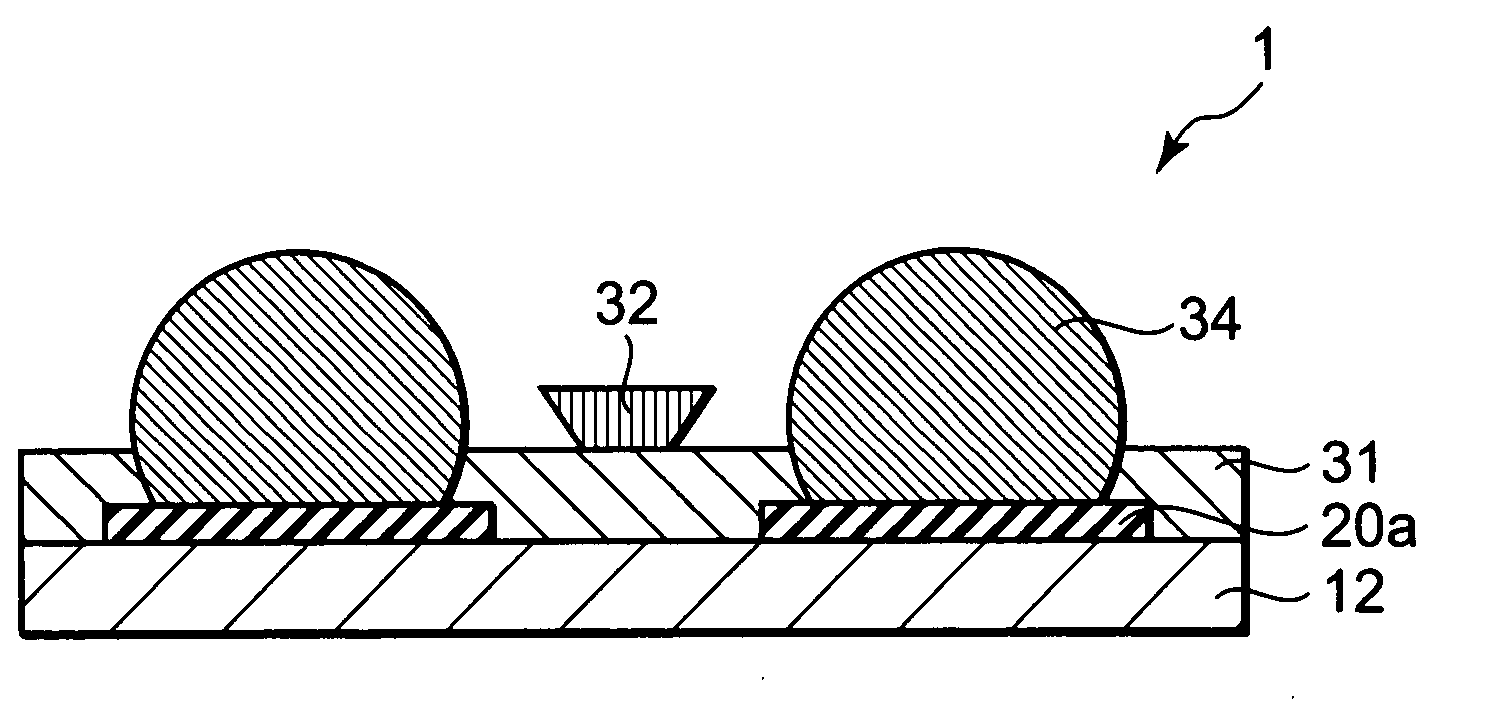
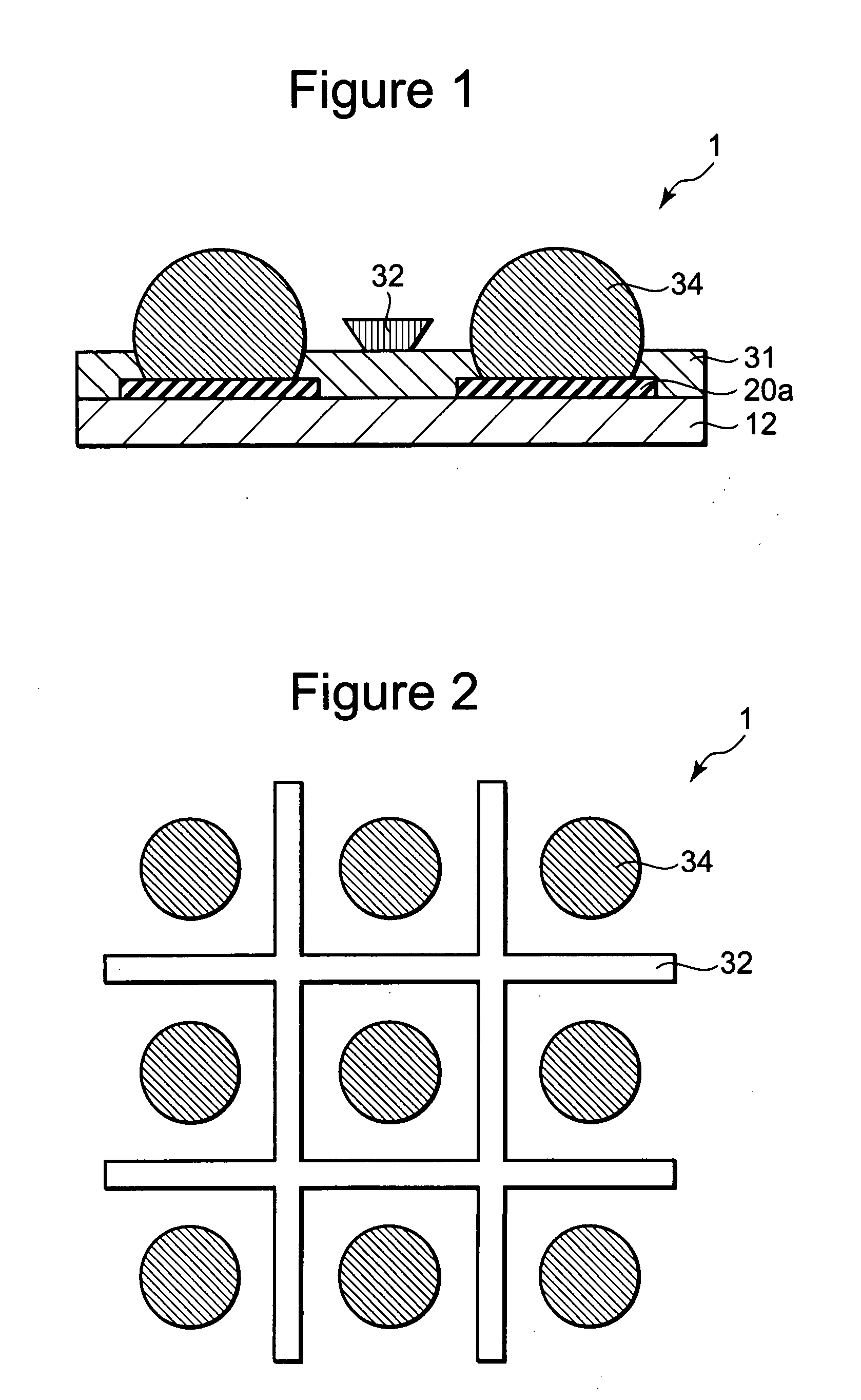
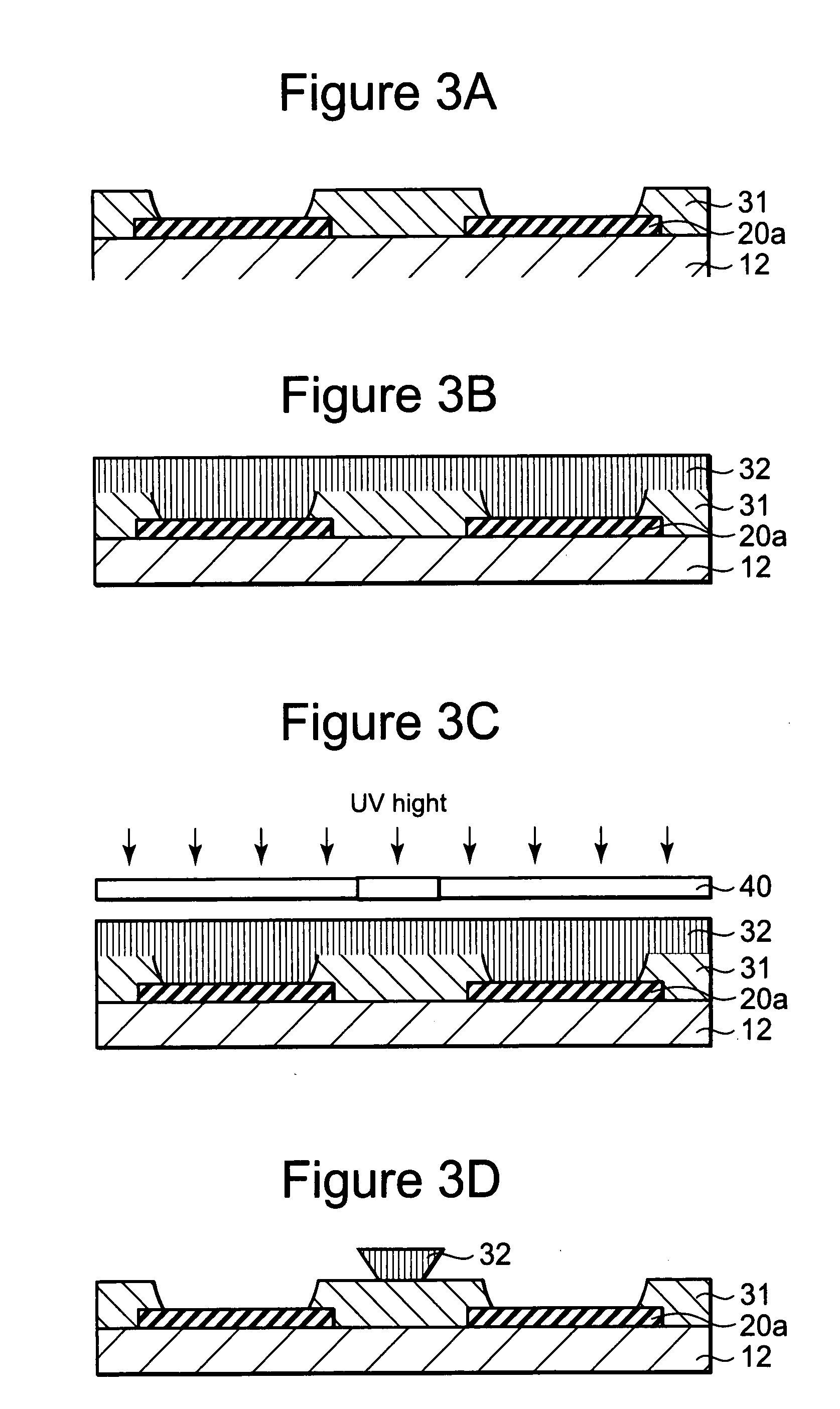
[0019]FIGS. 1 and 2 are a sectional view and a plan view, respectively, showing an outlined configuration of a printed wiring board according to the first embodiment of the present invention. A printed wiring board 1 is a printed wiring board on which electronic components are mounted via a solder bump 34, comprising a substrate main body 12, a solder resist layer 31 (first solder resist layer) provided on the substrate main body 12 and having a first opening in which a part of the solder bump 34 is buried, and a solder resist layer 32 (second solder resist layer) provided on the solder resist layer 31 and having a second opening through which the solder pump 34 extends. Here, the shape of the second opening is non-analogous, non-similar, or non-homothetic to the shape of the first opening when viewed as plane-wise. In this embodiment, the shapes of the first and second openings are circular and rectangular, respectively, when viewed as plane-wise. The first opening ...

Example

Second Embodiment

[0030]FIG. 4 is a plan view showing an outlined configuration of a printed wiring board according to the second embodiment of the present invention. In this connection, the structure of the section of a printed wiring board 2 is similar to that shown in FIG. 1. An opening (first opening) of a solder resist layer 31 is provided on a mounting pad 20a arranged in the form of a tetragonal lattice. In this embodiment, a solder resist layer 32 is formed as a dot pattern. Namely, the solder resist layer 32 is columnar. Its diameter is, for example, about 5 to 160 μm. In this embodiment, the solder resist layer 32 also has an undercut shape. Therefore, the solder resist layer 32 is tapered with the diameter gradually decreasing as going toward the solder resist layer 31. Furthermore, the solder resist layer 32 is arranged in the form of zigzag lattice with the first opening when viewed as plane-wise. Other aspects of the configuration and the production method for the print...


PUM

PropertyMeasurementUnit
Thicknessaaaaaaaaaa
Thicknessaaaaaaaaaa
Angleaaaaaaaaaa

Abstract

A printed wiring board includes: a substrate main body; a solder resist layer provided on the substrate main body and having a first opening in which a part of the solder bump is formed; and a solder resist layer provided on the solder resist layer and having a second opening through which the solder bump is formed. The shape of the second opening is non-analogous to the shape of the first opening when viewed as plane-wise.

Description

BACKGROUND OF THE INVENTION[0001]1. Field of the Invention[0002]The present invention relates to a printed wiring board and a method for production thereof.[0003]2. Description of Related Art[0004]As the speed has been enhanced and the number of pins has been increased for semiconductor devices, the proportion of application of C4 (Controlled Collapse Chip Connection) flip chip mounting has been increased among a various kinds of mounting methods. The C4 is a construction method of mounting a pad on a substrate with a pad on a chip by a solder bump. Furthermore, in this connection, for solders used in a bump material, demands for lead-free solders have grown in terms of environmental conservation. When the lead-free solder is used for both a wafer bump and a preliminary solder on a printed wiring board, the mounting temperature is high, and the entire bump is remelted at the time of reflow when a BGA solder ball is attached or when a semiconductor device is mounted on a board, as co...

Claims


Application Information

Patent Timeline
IPC IPC(8): H05K1/03B05C17/06
CPCH01L23/49816H01L2224/13021H01L2224/16H05K3/3452Y10T29/49155H05K2203/0588H05K2203/0594H01L2924/01322H05K2201/10674H01L2924/00014H01L2224/05599H01L2224/0555H01L2224/0556H01L2224/05573H01L2224/05567H01L2224/0554
Inventor ISHIDO, KIMINORI
Owner RENESAS ELECTRONICS CORP
Why Eureka
Try Eureka