Image sensor module

a technology of image sensor and module, which is applied in the field of image sensor, can solve the problems of reducing the yield rate during packaging process, damage to sensitive chips, and affecting the quality of the device, so as to reduce the size of the device, the effect of reducing the footprint and achieving the highest yield

Active Publication Date: 2008-06-12
ADVANCED CHIP ENG TECH
View PDF10 Cites 19 Cited by
  • Summary
  • Abstract
  • Description
  • Claims
  • Application Information

AI Technical Summary

Benefits of technology

[0012]In the present scheme, it is compatible with the COB, CSP type package, and the module can be linked to the mother board (MB) without the connector. Moreover, the present scheme may offers smaller foot print, it may reduce the device size. The solder joint terminal could be LGA, BGA. Further, the image sensor scheme may re-workable on the MB. The scheme may obtain highest yield during manufacturing in module / system assembly due to the protection layer is formed on the micro lens to avoid particle contamination during module assembly.

Problems solved by technology

If the unwanted particles are not removed from the sensor, it leads to downgrade the quality of the device.
In order to achieve the purpose, the removal by manual may damage the sensitive chip.
One drawback of the COB is lower yield rate during packaging process due to particle contamination on sensing area.
Besides, the drawbacks of the LCC are higher packaging cost and lower yield rate due to particle contamination on sensing area.
The transparency is bad due to epoxy wearing out, and the potential reliability may be reduced.

Method used


Image

  • Image sensor module
  • Image sensor module
  • Image sensor module

Examples


Embodiment Construction

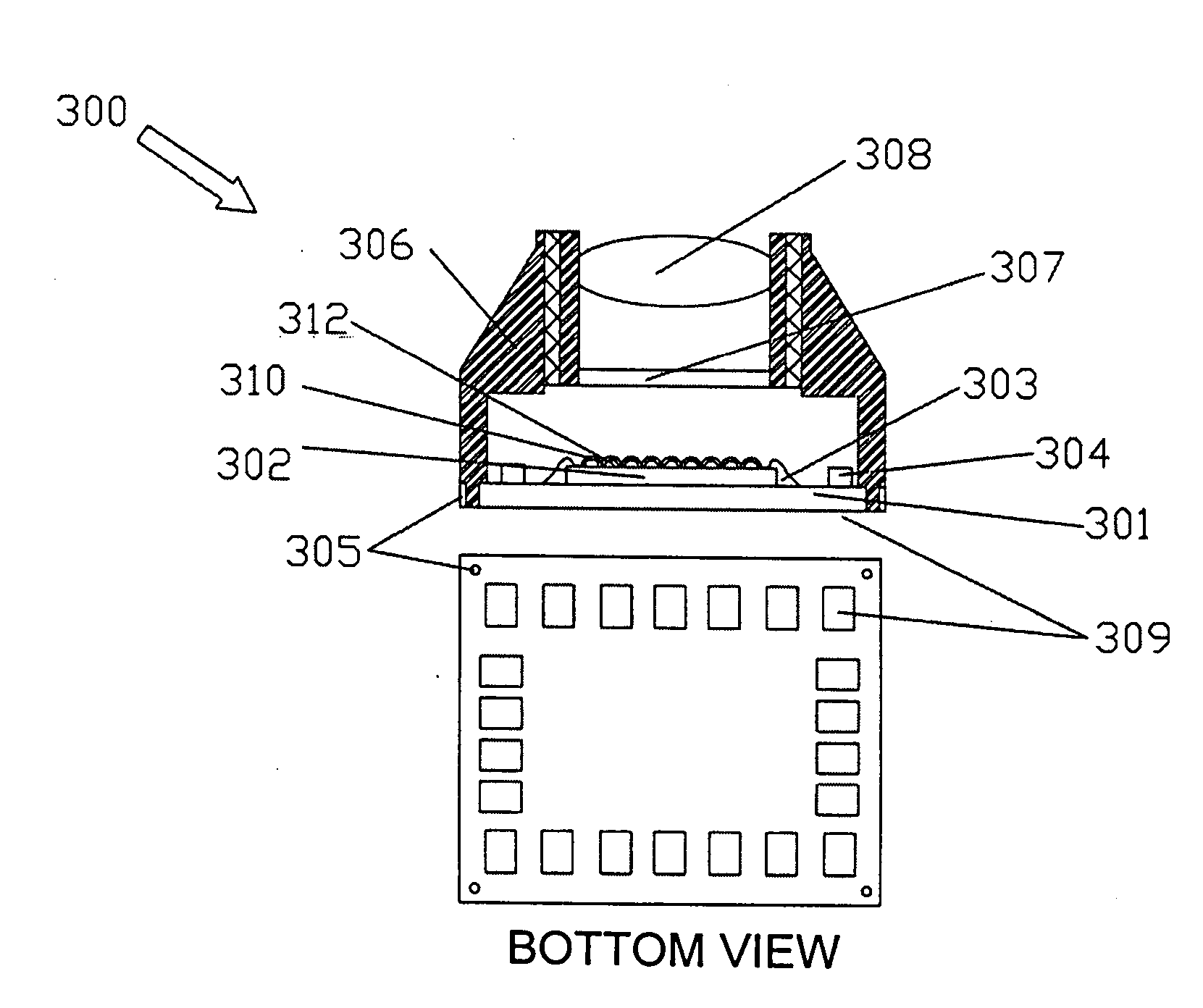
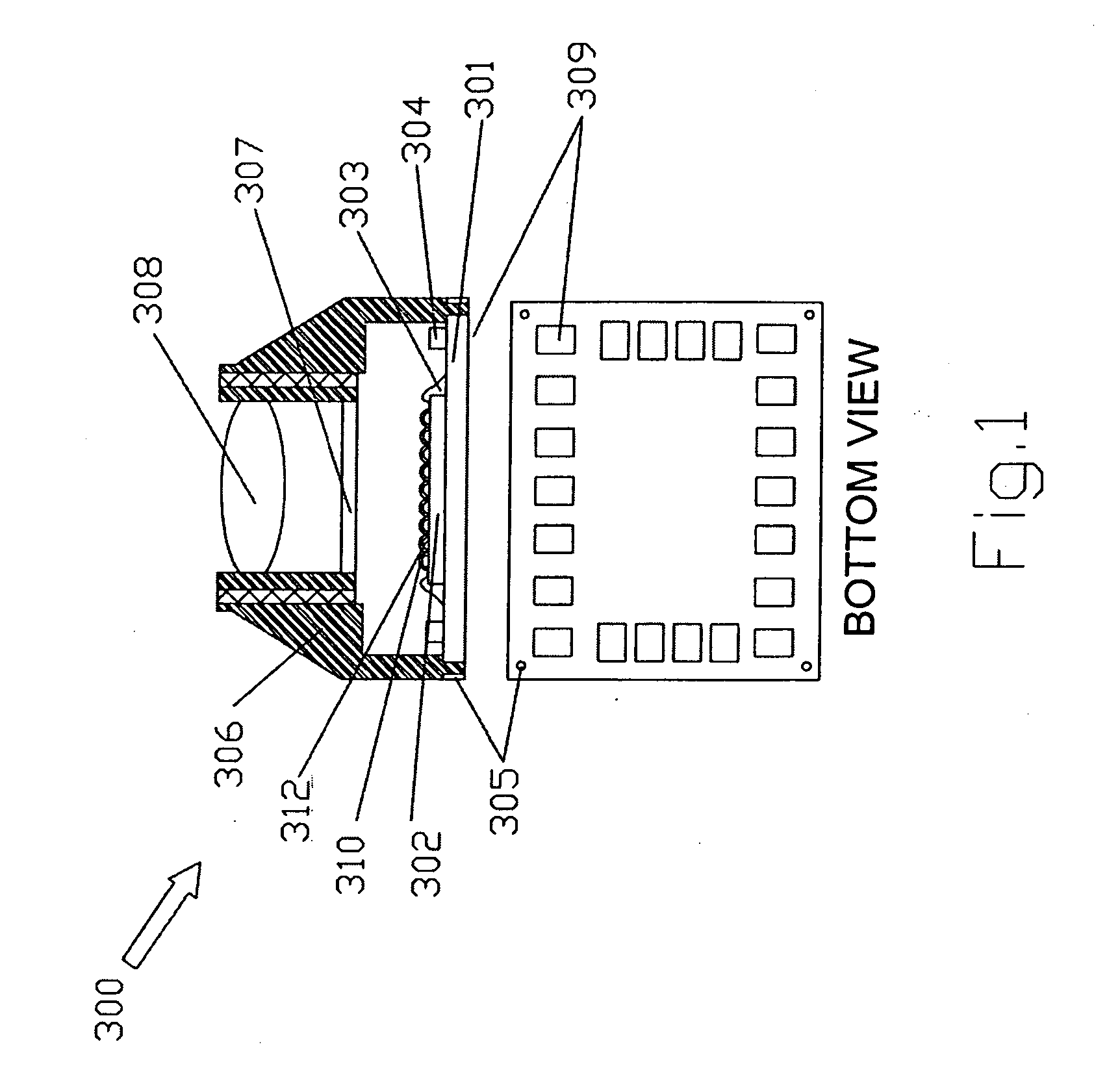
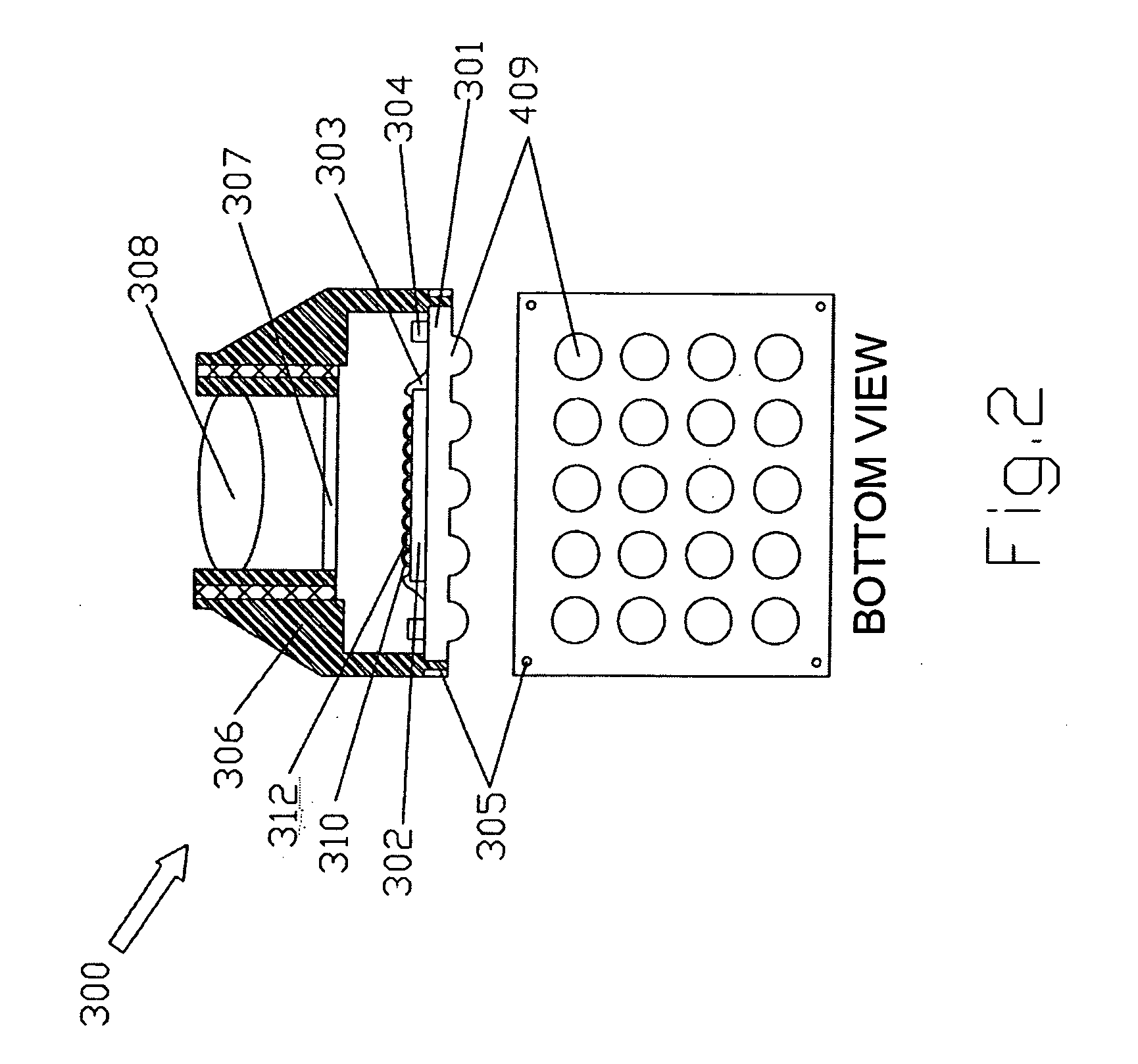
[0017]Some sample embodiments of the invention will now be described in greater detail. Nevertheless, it should be recognized that the present invention can be practiced in a wide range of other embodiments besides those explicitly described, and the scope of the present invention is expressly not limited except as specified in the accompanying claims. Then, the components of the different elements are not shown to scale. Some dimensions of the related components are exaggerated and meaningless portions are not drawn to provide clearer description and comprehension of the present invention. The structure is adaptable to the CSP (Chip Scale Package), FBGA (Fine-pitch Ball Grid Array) and COB (Chip On Board) type package. The present invention benefits lower cost and more simple process than the conventional die package. The present scheme may solve the cost issue suffered by conventional package. Further, data processing speed of the FBGA package is far faster than conventional TSOP ...


PUM


Abstract

The present invention provides an image sensor module. The image sensor module has a die formed on a substrate, the die having a micro lens area, a lens holder formed on the substrate and over the die, a lens formed in the lens holder. A filter is formed within the lens holder and between the lens and the die, and at least one passive device formed on the substrate and covered within the lens holder. Conductive bumps or LGA (leadless grid array) are formed on the bottom surface of the substrate.

Description

BACKGROUND OF THE INVENTION[0001]1. Field of the Invention[0002]This invention relates to an image sensor, and more particularly to an image sensor module and the method of forming the same.[0003]2. Description of the Prior Art[0004]With the spread of digital cameras, a demand for solid imaging devices has risen in recent years. The attention has recently been riveted to CMOS image sensors which can be manufactured by complementary metal-oxide semiconductors (CMOS) technology, and the unit cost of the production of which is low. The pixel section of the CMOS image sensor includes a plurality of unit pixels arranged in the form of a matrix. Each of the unit pixels includes a photodiode and a readout transistor configured to read out signal charges accumulated in the photodiode. A gate voltage generator is connected to a gate electrode of the readout transistor. A select switch switches a voltage applied to the gate electrode so as to turn on and off the readout transistor.[0005]As af...

Claims


Application Information

Patent Timeline
Patent Type & Authority Applications(United States)
IPC IPC(8): H01L27/00
CPCH01L27/14618H04N5/2251H04N5/2257H01L2924/0002H01L2224/48091H01L2924/00H01L2924/00014H01L27/14627H04N23/57H04N23/55H01L27/146
Inventor YANG, WEN-KUNCHANG, JUI-HSIEN
Owner ADVANCED CHIP ENG TECH
Why Eureka
Try Eureka