Germanium semiconductor device and method of manufacturing the same

a technology of germanium semiconductor and manufacturing method, which is applied in the direction of semiconductor devices, electrical devices, transistors, etc., can solve the problems of difficult manufacturing of ge mos transistors, poor economical efficiency and reproducibility, and many process difficulties, so as to improve the driving current characteristic of the device, reduce contact resistance, and rapid thermal annealing

a technology of germanium semiconductor and manufacturing method, which is applied in the direction of semiconductor devices, electrical devices, transistors, etc., can solve the problems of difficult manufacturing of ge mos transistors, poor economical efficiency and reproducibility, and many process difficulties, so as to improve the driving current characteristic of the device, reduce contact resistance, and rapid thermal annealing

US20080135878A1Inactive Publication Date: 2008-06-12ELECTRONICS & TELECOMM RES INST +1

Image

  • Germanium semiconductor device and method of manufacturing the same
  • Germanium semiconductor device and method of manufacturing the same
  • Germanium semiconductor device and method of manufacturing the same

Examples


Embodiment Construction

[0023]The present invention will now be described more fully hereinafter with reference to the accompanying drawings, in which exemplary embodiments of the present invention are shown.

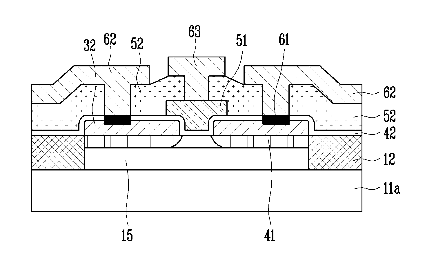
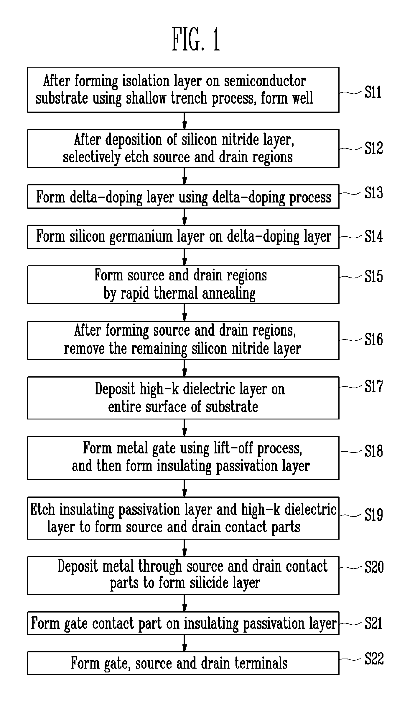
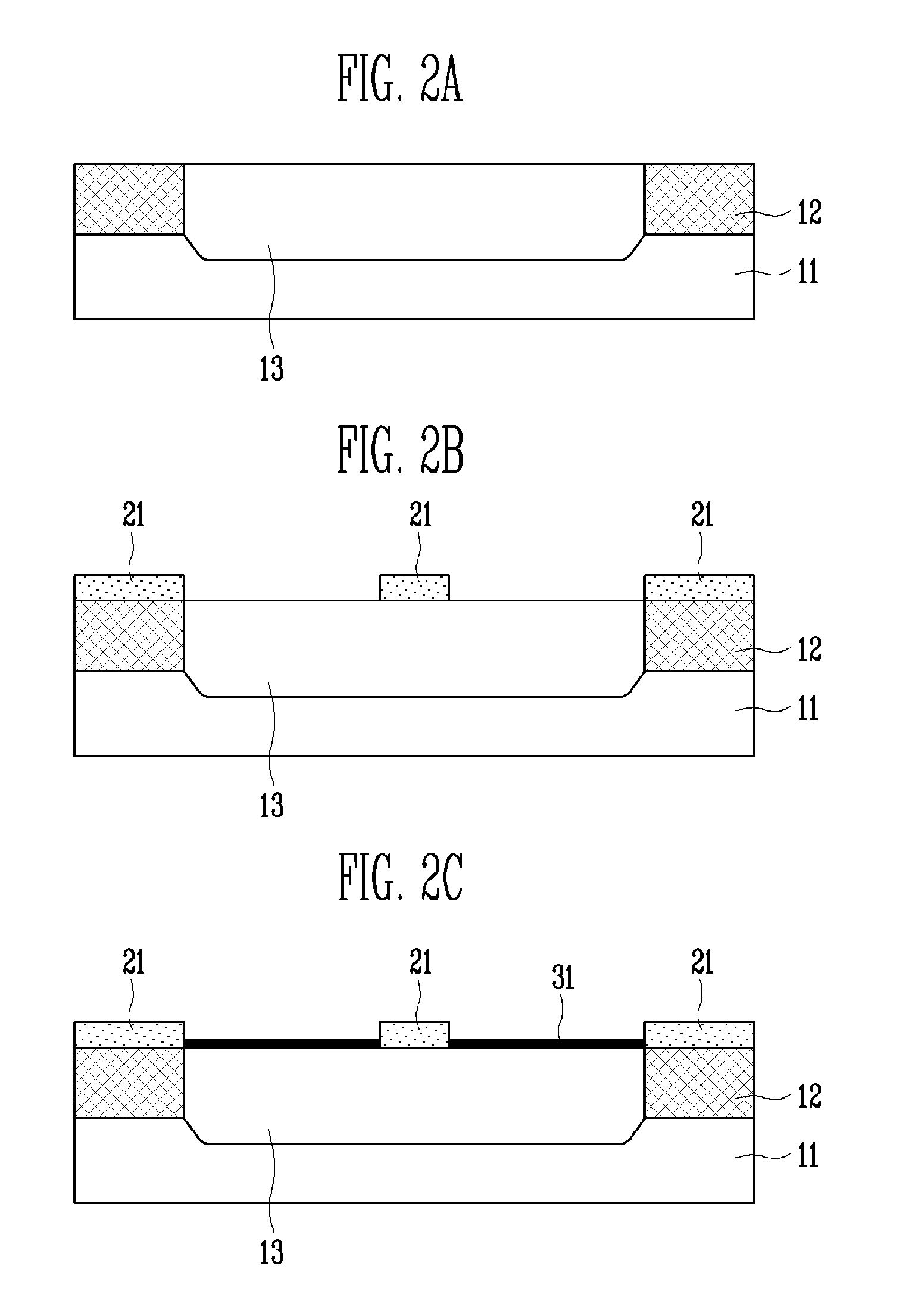
[0024]FIG. 1 is a flowchart illustrating a method of manufacturing a germanium (Ge) semiconductor device according to an exemplary embodiment of the present invention, and FIGS. 2A to 2H are cross-sectional views illustrating a method of manufacturing a Ge semiconductor device having source and drain regions according to an exemplary embodiment of the present invention.

[0025]To manufacture the Ge semiconductor device according to the present invention, referring to FIGS. 1 (S11) and 2A, an isolation layer 12 is formed on a semiconductor substrate 11 using a shallow trench process, and then a well 13 is formed thereon by ion injection. Here, the semiconductor substrate 11 may be a single crystal Ge substrate or a high-quality Ge on insulator (GOI) substrate based on a silicon substrate.

[0026]Referring t...


PUM

PropertyMeasurementUnit
temperatureaaaaaaaaaa
gate widthaaaaaaaaaa

Abstract

A germanium semiconductor device and a method of manufacturing the same are provided. The method includes the steps of: forming an isolation layer on a substrate using a shallow trench; forming a silicon-nitride layer on the substrate, and selectively etching the silicon nitride layer to expose source and drain regions; injecting impurities onto a surface of the substrate over the exposed source and drain regions using delta-doping to form a delta-doping layer; selectively growing a silicon germanium layer containing impurities on the delta-doping layer; rapidly annealing the substrate and forming source and drain regions by diffusion of the impurities; depositing an insulating layer on the entire surface of the substrate; etching the insulating layer and forming source and drain contact parts to be in contact with source and drain terminals; depositing metal over the insulating layer having the source and drain contact parts thereon and forming a metal silicide layer; and after forming the silicide layer, forming the source and drain terminals to be in contact with the silicide layer. Accordingly, the source and drain regions having a shallow junction depth may be ensured by forming the source and drain regions through annealing after delta-doping and selectively growing the silicon germanium layer containing high-concentration impurities. Also, the germanium silicide layer is stably formed by the silicon germanium layer grown in the source and drain regions, and thus contact resistance is lowered and driving current of the device is improved.

Description

CROSS-REFERENCE TO RELATED APPLICATION[0001]This application claims priority to and the benefit of Korean Patent Application Nos. 2006-123137, filed on Dec. 6, 2006 and 2007-20057 filed on Feb. 28, 2007, the disclosures of which are incorporated herein by reference in their entirety.BACKGROUND[0002]1. Field of the Present Invention[0003]The present invention relates to a germanium semiconductor device and a method of manufacturing the same, and more particularly, to a germanium semiconductor device comprising source and drain regions in a germanium substrate formed by delta-doping, in-situ selective deposition of a silicon-germanium (SiGe) layer containing impurities and diffusion through annealing, and a method of manufacturing the same.[0004]2. Discussion of Related Art[0005]With the trend to various compact, thin and lightweight electrical devices, the scaling-down of a semiconductor device has recently been accelerated. As a CMOS transistor is reduced in size, the device increas...

Claims


Application Information

Patent Timeline
12 Jun 2008
Publication
US20080135878A1
IPC
H01L21/336; H01L29/78
CPC
H01L21/223; H01L21/28079; H01L29/165; H01L29/41783; H01L29/517; H01L29/78684; H01L29/66545; H01L29/66606
Inventors
KIM, SANG HUN; BAE, HYUN CHEOL