Semiconductor memory device

a memory device and semiconductor technology, applied in semiconductor devices, digital storage, instruments, etc., can solve the problems of further complicated dram process, inability to scale capacitors, and increase process costs, and achieve the effect of fast access

Inactive Publication Date: 2008-06-12
RENESAS ELECTRONICS CORP
View PDF3 Cites 27 Cited by
  • Summary
  • Abstract
  • Description
  • Claims
  • Application Information

AI Technical Summary

Benefits of technology

[0036]A time for restoring charges into the memory c...

Problems solved by technology

In the DRAM cell, therefore, the size of the transistor can be reduced according to the scaling rule, but the scaling of the capacitor is impossible.
Therefore, a further complicated DRAM process is required for scaling the memory cell in the large-capacity, dual-port RAM of the DRAM cell type disclosed in the articles 1 and 2.
This results in a problem of further increase in process cost.
In the DRAM-cell-type, dual-port RAM cell, destructive read is performed, and thus data reading destroys storage data of the memory cell.
When the memory cell at the same address is simultaneously access via the two ports, for example, the stored charges in the memory cell capacitor of the DRAM cell disperse to the two ports, so that a read voltage lowers, and a read failure may occur.
Therefo...

Method used


Image

  • Semiconductor memory device
  • Semiconductor memory device
  • Semiconductor memory device

Examples


first embodiment

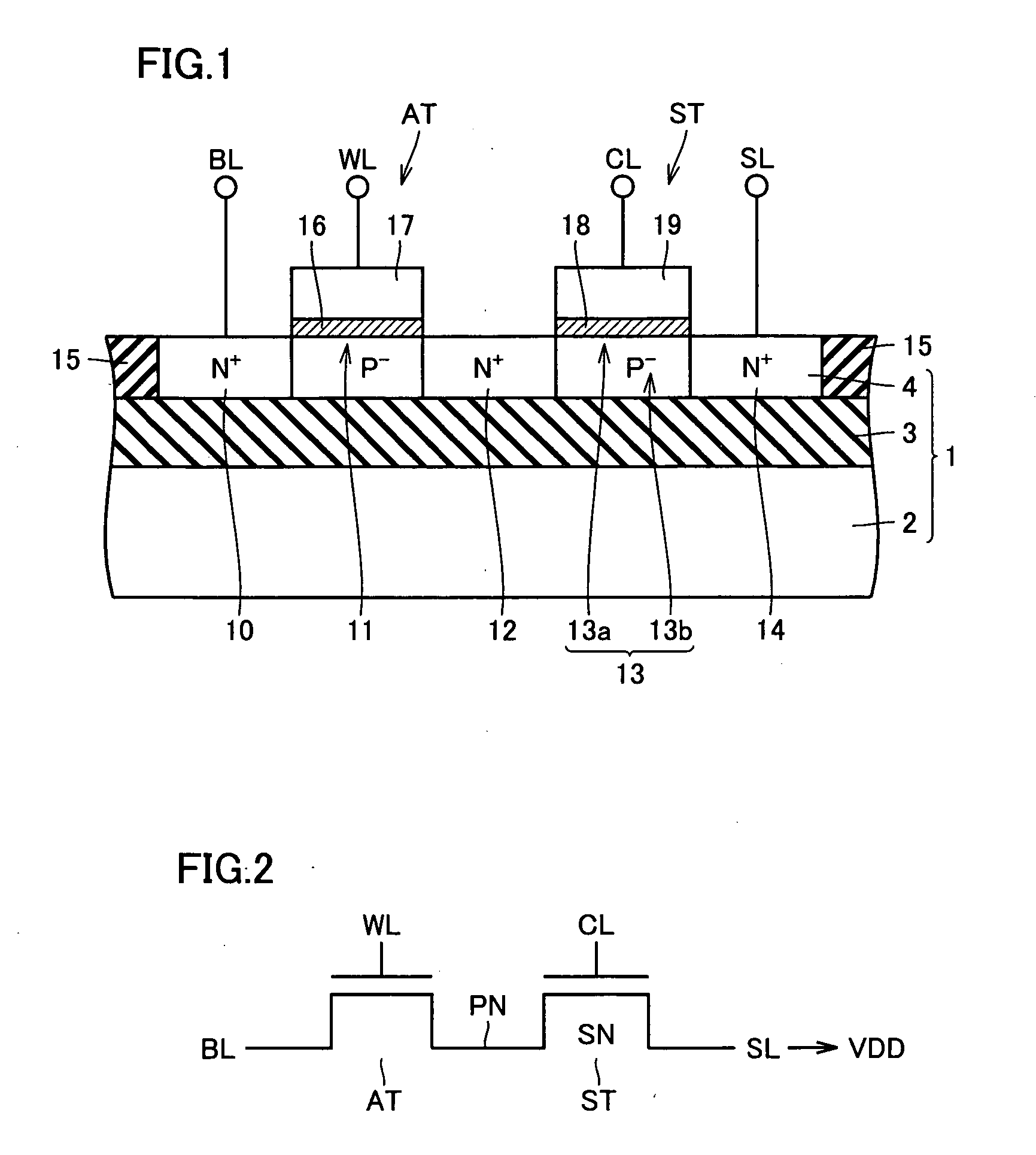
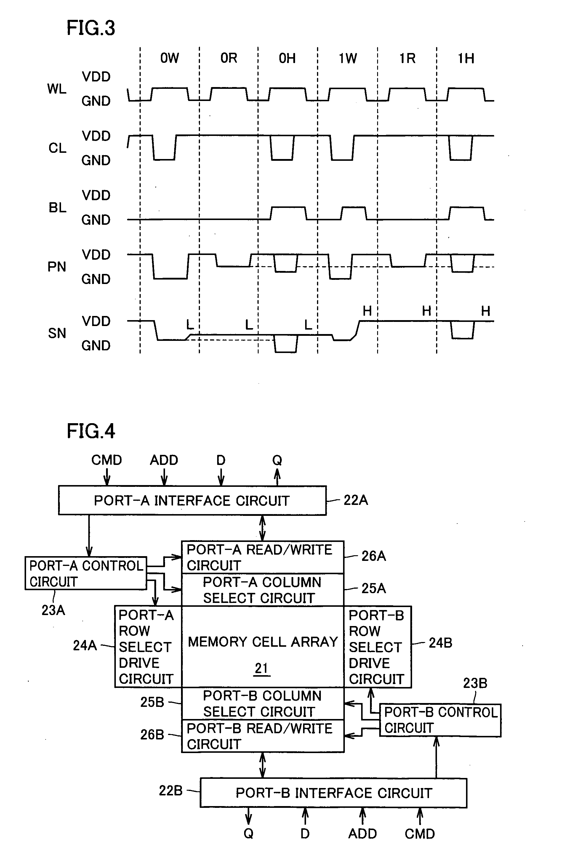
[0134]FIG. 4 schematically shows a whole configuration of a semiconductor memory device (which will be referred to as a “dual-port RAM” hereinafter) according to a first embodiment of the invention. In FIG. 4, dual-port RAM includes a memory cell array 21 having memory cells (not shown) arranged in rows and columns. In memory cell array 21, there are provided dual-port cells each allowing access from two ports A and B as will be described later. The dual-port cell is formed with the TTRAM cell being a base.

[0135]The dual-port RAM further includes port-A and port-B interface circuits 22A and 22B for accessing from the ports A and B, respectively. The “port” indicates a portion through which access of data is performed. Therefore, when reference is made to the whole memory, the “port” indicates the input / output portion for signal / data coupled to a data bus. When the wording “port” is used in connection with the memory cell, it indicates a portion through which write / read of data is pe...

second embodiment

[0182]FIG. 12 schematically shows a planar layout of a memory cell array of a semiconductor memory device according to a second embodiment of the invention. FIG. 12 representatively shows memory cells arranged in two rows and three columns.

[0183]In FIG. 12, rectangular active regions 50a, 50b and 50c are aligned in the X direction with spaces in between. Active regions 50d and 50e are aligned in the X direction with a space in between. Active regions 50a-50c are displaced in the X direction from active regions 50d and 50e by half a column.

[0184]In the memory cell row, second metal interconnections 51a and 51b are arranged on the opposite ends in the Y direction, respectively. These second metal interconnections 51a and 51b form source lines SL1 and SL2, respectively. Source lines SL1 and SL2 have regions coupled to a global source line although not shown, and receive the power supply voltage. Second metal interconnection 51a is electrically connected through source via / contacts SCTa...

third embodiment

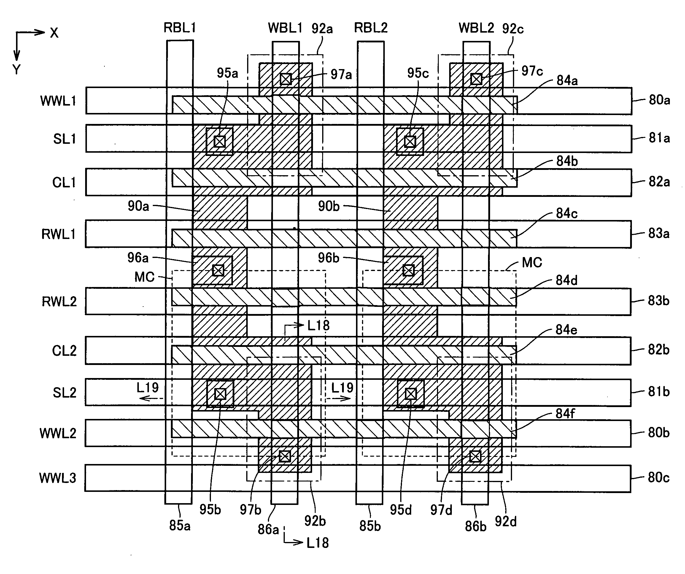
[0227]FIG. 17 schematically shows a planar layout of a memory cell array of a semiconductor memory device according to a third embodiment of the invention. In FIG. 17, second metal interconnections 80a, 81a, 82a and 83a are arranged continuously extending in the X direction with spaces in between. Second metal interconnection 80a forms a write word line WWL1, and second metal interconnection 81a forms source line SL1. Second metal interconnections 82a forms charge line CL1, and second metal interconnection 83a forms a read word line RWL1.

[0228]Second metal interconnections 83b, 82b, 81b, 80b and 80c are arranged continuously extending in the X direction with spaces in between. Second metal interconnection 83b forms a read word line RWL2, second metal interconnection 82b forms charge line CL2 and second metal interconnection 81b forms charge line SL2. Second metal interconnection forms a write word line WWL2, and second metal interconnection 80c forms a write word line WWL3.

[0229]A p...


PUM


Abstract

One memory cell is formed of a first port access transistor, a second port access transistor and a storage transistor coupled commonly to these access transistors. The first port access transistor is coupled to a first electrode of the storage transistor, and the second port access transistor is coupled to a third electrode of the storage transistor. These first and second port access transistors enter a selected state when first and second port word lines are selected, respectively, to couple corresponding second and third electrodes of the corresponding storage transistor to first and second port bit lines, respectively. A dual-port memory cell of which scalability can follow miniaturization in a process can be provided.

Description

BACKGROUND OF THE invention[0001]1. Field of the Invention[0002]The present invention relates to a semiconductor memory device, and particularly to a semiconductor memory device including transistors of an SOI (Silicon On Insulator) structure formed on an insulating film. Specifically, the present invention relates to an arrangement of a memory cell array in a multiport semiconductor memory device that can be accessed via multiple ports.[0003]2. Description of the Background Art[0004]In fields of image data processing and the like, system LSIs in which a logic such as a processor and a memory device are integrated on a single semiconductor chip have been widely used for high-speed processing of a large amount of data. In these system LSIs, the logic and the memory device are interconnected via on-chip interconnection lines, so that the following advantages can be achieved.[0005](1) A load on a signal line is smaller than that on an on-board interconnection line, and data and signals...

Claims


Application Information

Patent Timeline
IPC IPC(8): G11C5/06
CPCG11C5/063G11C7/12G11C7/18G11C8/16G11C11/405G11C11/4094H01L29/7841G11C2211/4016H01L21/84H01L27/0207H01L27/108H01L27/10802H01L27/1203G11C11/4097H10B12/20H10B12/00
Inventor SHIMANO, HIROKIMORISHITA, FUKASHIARIMOTO, KAZUTAMI
Owner RENESAS ELECTRONICS CORP
Why Eureka
Try Eureka