Coatings for components of semiconductor wafer fabrication equipment

Inactive Publication Date: 2008-06-12
COORSTEK INC
View PDF5 Cites 32 Cited by
  • Summary
  • Abstract
  • Description
  • Claims
  • Application Information

AI Technical Summary

Benefits of technology

[0005]Embodiments of the invention include methods of forming a high wear resistance coating on a substrate having a low coefficient of thermal expansion. The methods may include the step of providing the low CTE substrate, where a surface of the subs

Problems solved by technology

In operation, the slightest temperature gradients generated by the environment or process can have detrimental effects on the process quality due to the substrate and substrate support thermally generated expansion.
The sensitivity to slight temperature gradients causing sub-micron dimensional and geometric tolerances can limit the materials used to make the wafer support to materials with relatively low thermal expansion characteristics over the temperature range of operation.
Unfortunately, some of the

Method used


Image

  • Coatings for components of semiconductor wafer fabrication equipment
  • Coatings for components of semiconductor wafer fabrication equipment
  • Coatings for components of semiconductor wafer fabrication equipment

Examples


Embodiment Construction

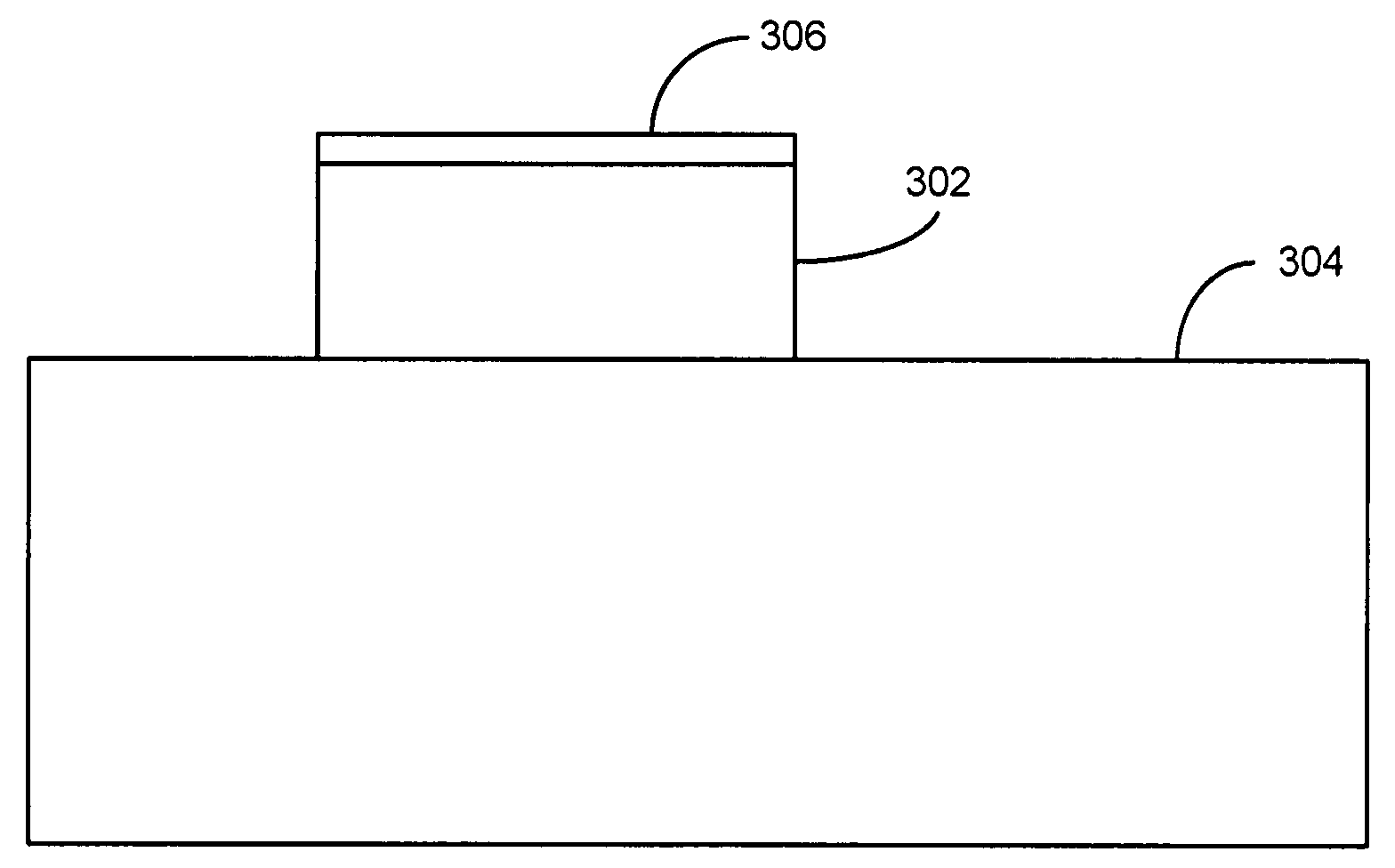
[0019]The present invention relates to wafer support components (e.g., a wafer chuck) for wafer fabrication devices, and methods of making those components. The wafer support components are made from a substrate with raised protrusions that contact and support a precise position of the wafer during a wafer processing operation. The substrate includes one or more materials having low coefficients of thermal expansion (CTEs) that do not significantly expand and / or contract during a processing operation. Because many of the low CTE substrate materials used are relatively soft and can wear down rapidly (e.g., 2-3 months) during repeated use, a high wear resistance layer is formed on the protrusions to reduce the wear rate of the component. A high wear resistance layer is a layer having a solid surface that resists erosion and / or dimensional change from frictional contact with another solid surface. The high wear resistance layer can extend the lifetime of a wafer support component by tw...


PUM

PropertyMeasurementUnit
Temperatureaaaaaaaaaa
Lengthaaaaaaaaaa

Abstract

A method of forming a high wear resistance coating on a substrate having a low coefficient of thermal expansion is described. The method may include providing the low CTE substrate, where a surface of the substrate includes a plurality of protrusions raised above the surface. A high wear resistance layer is formed on a top portion of protrusions, where the layer is not contiguous between adjacent protrusions on the substrate. Also, a wafer support component to support a wafer during, for example, a photolithography or inspection process. The wafer support component includes a substrate that has a material with a low coefficient of thermal expansion, where the substrate has a surface with a plurality of protrusions raised about the surface. A high wear resistance layer is formed on a top surface of each of the protrusions.

Description

CROSS-REFERENCES TO RELATED APPLICATIONS[0001]This application claims the benefit of U.S. Provisional Application No. 60 / 869,202, filed Dec. 8, 2006, entitled “COATINGS FOR COMPONENTS OF SEMICONDUCTOR WAFER FABRICATION EQUIPMENT,” the entire contents of which is herein incorporated by reference for all purposes.BACKGROUND OF THE INVENTION[0002]Integrated circuit chip fabrication generally involves printing features on a substrate wafer using photolithography techniques. During the photolithography process, the position of the wafer substrate relative to imaging system needs to be very precise, requiring the substrate support to be built and maintained to sub-micron tolerances. In operation, the slightest temperature gradients generated by the environment or process can have detrimental effects on the process quality due to the substrate and substrate support thermally generated expansion. The sensitivity to slight temperature gradients causing sub-micron dimensional and geometric to...

Claims


Application Information

Patent Timeline
IPC IPC(8): B05D5/12B05C13/00
CPCC23C14/048H01L21/68757H01L21/6875
Inventor WILLIAMS, STEVEN C.
Owner COORSTEK INC
Why Eureka
Try Eureka