
Semiconductor manufacturing process

a technology of semiconductors and manufacturing processes, applied in the direction of cleaning processes and apparatus, semiconductor devices, chemistry apparatus and processes, etc., can solve problems such as process defects

Active Publication Date: 2008-06-19
UNITED MICROELECTRONICS CORP
View PDF31 Cites 21 Cited by
  • Summary
  • Abstract
  • Description
  • Claims
  • Application Information

AI Technical Summary

Benefits of technology

[0010]It is a main object of the present invention to provide a semiconductor manufacturing process, which is capable of avoiding formation of precipitates on a substrate surface to lead a process defect in an etching process employing a hard mask.
[0012]In the semiconductor manufacturing process according to the present invention, after etching the underlying layer beneath the hard mask with fluorine radical-containing plasma using a hard mask, such as Ti / TiN hard mask, a treatment (or post-treatment) is carried out using a gas reactive to fluorine radicals to react with residual fluorine radicals. A fluorine-containing compound is thus formed and removed. Thus, the process defect caused by the titanium-fluorine compound precipitates formed on the substrate surface through the reaction of fluorine radicals with, for example, titanium, contained in the hard mask as that in the prior art can be prevented.

Problems solved by technology

However, using a fluoroalkane plasma, such as CH2F2 or CHF3 plasma, to remove the cap layer 14 in the aforesaid etching step may lead to a process defect due to the formation of titanium-fluorine compound precipitates on the substrate surface through the reaction of fluorine radicals with the titanium contained in the hard mask.
It is not desired and is a problem needed to solve.

Method used


Image

  • Semiconductor manufacturing process
  • Semiconductor manufacturing process
  • Semiconductor manufacturing process

Examples


Embodiment Construction

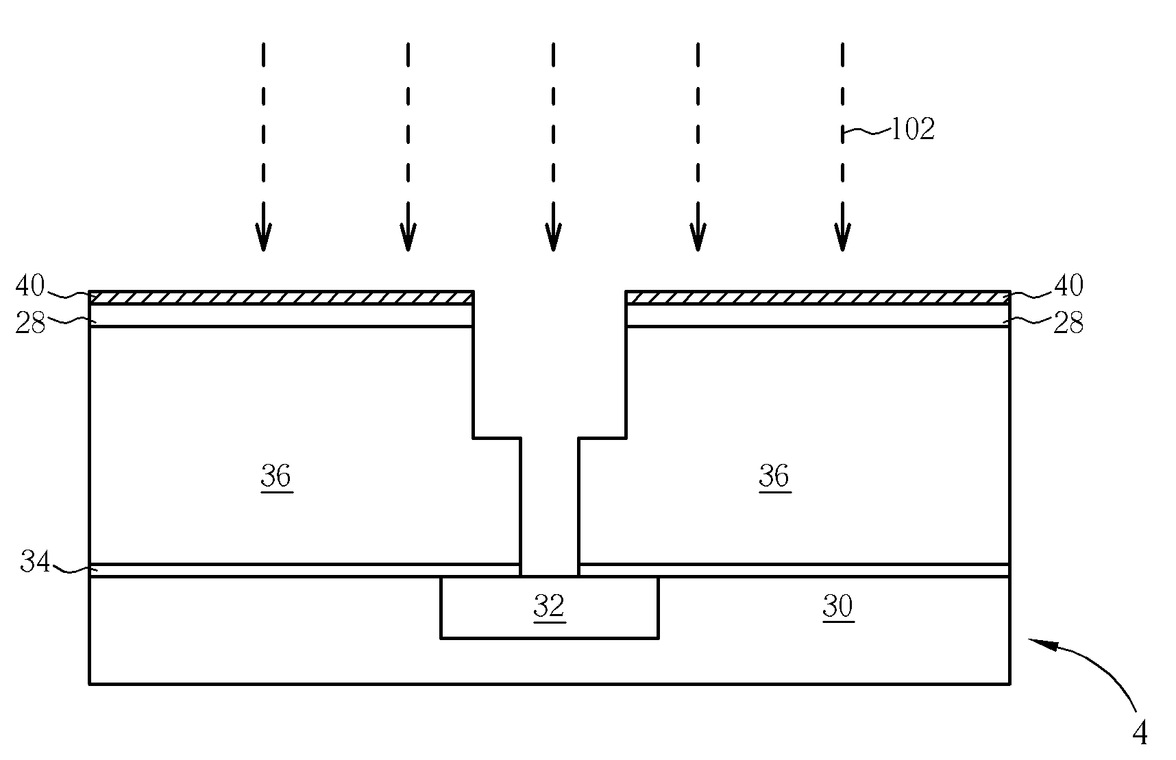
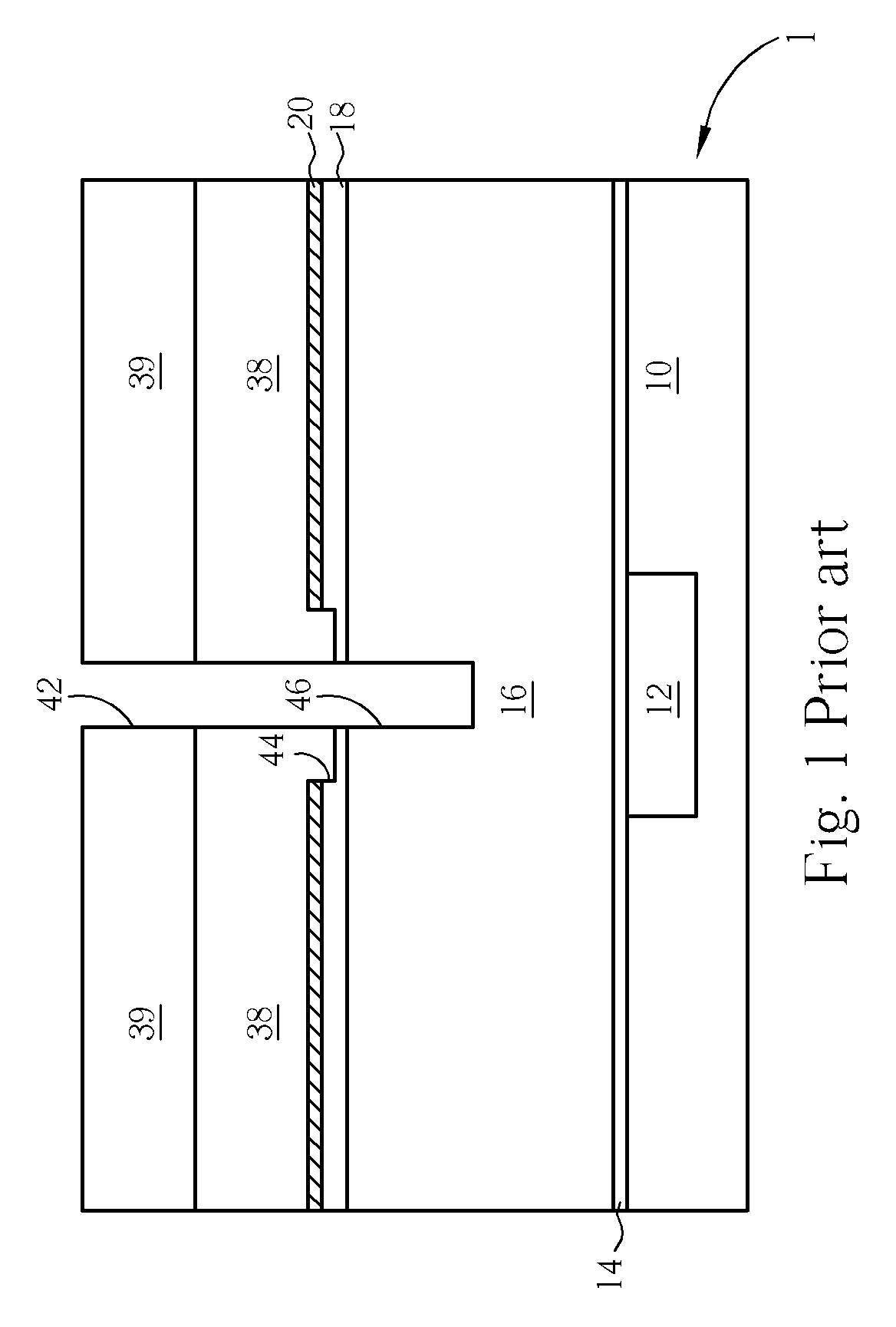
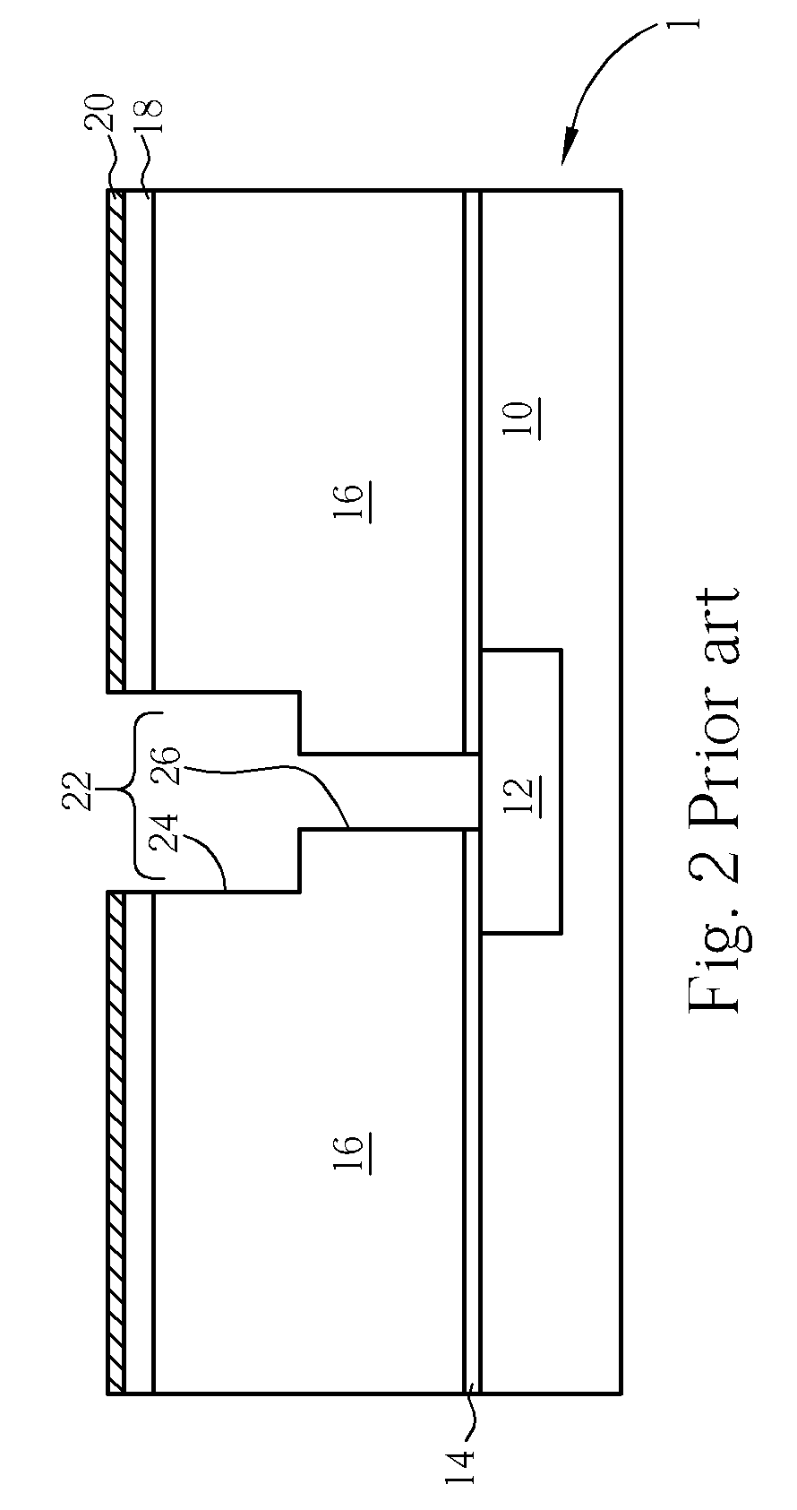
[0020]Please refer to FIGS. 3 and 4, schematic, cross-sectional diagrams showing an embodiment of the semiconductor manufacturing process according to the present invention. The embodiment is illustrated with a damascene process. In the drawings, like numeral numbers designate like elements, regions or layers. It is understood that the present invention is not limited to the embodiments illustrated in the drawings. The process of the present invention may be suited in any process as long as a hard mask, especially a hard mask containing titanium component, such as Ti metal or TiN, and fluorine radical containing gas for etching are used in the process. The process may be, for example, a damascene process or a dual damascene process, but not limited thereto. The damascene process may be a trench-first damascene, a via-first damascene, or a partial via-first damascene processes, among others.

[0021]As shown in FIG. 3, a substrate 2, which may be a semiconductor substrate, having thereo...


PUM

PropertyMeasurementUnit
thicknessaaaaaaaaaa
thicknessaaaaaaaaaa
thicknessaaaaaaaaaa

Abstract

Disclosed is a semiconductor manufacturing process, in which a fluorine radical-containing plasma is used to etch a hard mask and a layer therebeneath; and a treatment is carried out using a gas reactive to fluorine radicals for reacting with residual fluorine radicals to form a fluorine-containing compound and remove it. Thus, precipitates formed by the reaction of fluorine radicals and titanium components existing in the hard mask to cause a process defect can be avoided.

Description

BACKGROUND OF THE INVENTION[0001]1. Field of the Invention[0002]The invention relates to a semiconductor manufacturing process, and more particularly, to a process using a hard mask comprising metal during a semiconductor process.[0003]2. Description of the Prior Art[0004]With the progress of the semiconductor industry, the devices of integrated circuits have been reduced in size under sub-micron for development and design of high-density integrated circuits. In semiconductor manufacturing processes, mask technology is frequently utilized.[0005]For example, integrated circuit fabrication on semiconductor structures for ultra scale integration (ULSI) requires multiple levels of metal interconnections for electrically connecting the miniaturized semiconductor devices. To overcome difficulties in fabricating metal interconnection in multi-layer, the damascene structure has been extensively researched and developed. In addition, because the resistive coefficient of copper is lower than ...

Claims


Application Information

Patent Timeline
Patent Type & Authority Applications(United States)
IPC IPC(8): H01L21/3065
CPCH01L21/02063H01L21/31116H01L21/76814H01L21/76811H01L21/31144Y10S438/906Y10S438/963
Inventor LAI, YU-TSUNGHUANG, CHUN-JENYAU, JYH-CHERNGLIAO, JIUNN-HSIUNG
Owner UNITED MICROELECTRONICS CORP
Learn More