Check patentability & draft patents in minutes with Patsnap Eureka AI!

Buffer circuit

a buffer circuit and circuit technology, applied in logic circuit coupling/interface arrangement, pulse technique, baseband system details, etc., can solve the problems of reducing system efficiency, consuming more power, complex circuit design, etc., and reducing system efficiency. , the effect of reducing the efficiency of the system

Inactive Publication Date: 2008-06-26
IND TECH RES INST
View PDF52 Cites 4 Cited by
  • Summary
  • Abstract
  • Description
  • Claims
  • Application Information

AI Technical Summary

Benefits of technology

[0006]Although an analog buffer circuit may provide high efficiency in certain applications, such circuit has complicated designs, consumes more power, and requires large circuit areas. Thus, some systems use digital circuits instead to reduce power consumption and circuit area. However, digital circuits may suffer from poor noise tolerance. In addition, when digital circuits operate in high frequency, the resulting switching noise may decrease the system efficiency.

Problems solved by technology

Although an analog buffer circuit may provide high efficiency in certain applications, such circuit has complicated designs, consumes more power, and requires large circuit areas.
However, digital circuits may suffer from poor noise tolerance.
In addition, when digital circuits operate in high frequency, the resulting switching noise may decrease the system efficiency.

Method used


Image

  • Buffer circuit
  • Buffer circuit
  • Buffer circuit

Examples


Embodiment Construction

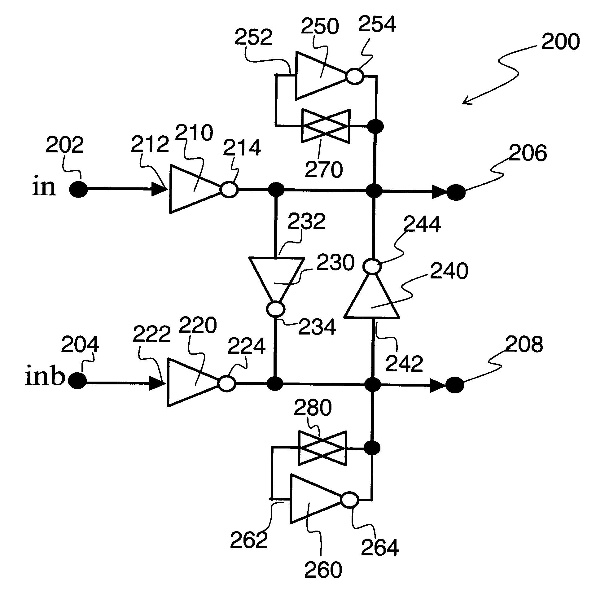
[0024]FIG. 2 illustrates an exemplary circuit diagram of a buffer circuit 200 in examples consistent with the present invention. The buffer circuit may have a first input terminal 202, a second input terminal 204, a first output terminal 206 and a second output terminal 208. The first input terminal 202 may be coupled to an input signal Vin. The first output terminal 206 may provide an output signal Vout. The second input terminal 204 may be coupled to a complementary input signal Vin*, in which case the terminal 208 is used as a complementary output terminal to provide a complementary output signal Vout*. Alternatively, the second input terminal 204 may be coupled to a reference voltage Vref, in which case the output at the terminal 208 is usually not used.

[0025]Referring to FIG. 2, the buffer circuit 200 includes a differential pair which receives input signals and generates amplified signals from the input signals. The differential pair may enhance signal driving capability as we...


PUM


Abstract

A buffer circuit having an input terminal and an output terminal comprises a first inverter having an input node coupled to the input terminal and an output node coupled to the output terminal, a second inverter having an input node coupled to a reference voltage and an output node, a third inverter having an input node coupled to the output terminal and an output node coupled to the output node of the second inverter, a fourth inverter having an input node coupled to the output node of the second inverter and an output node coupled to the output terminal, a fifth inverter having an input node and an output node coupled to the output terminal, a sixth inverter having an input node and an output node coupled to the output node of the second inverter, a first resistive element is coupled between the output terminal and the input node of the fifth inverter, and a second resistive element is coupled between the output node of the second inverter and the input node of the sixth inverter.

Description

BACKGROUND OF THE INVENTION[0001]1. Field of the Invention[0002]This invention relates to a buffer circuit, and more particularly, to a buffer circuit that may be used in digital devices or systems.[0003]2. Background of the Invention[0004]Buffers are commonly used in data transmission systems. For example, a signal buffer circuit may be used at an input interface to receive or amplify signals, enhance signal driving capability, and / or reduce signal transition time.[0005]Buffer circuits are usually designed using analog circuits. An example of an analog buffer circuit may include a differential pair with various passive elements, including inductors, capacitors and resistors. FIG. 1A shows an analog buffer circuit 100A for Pseudo Emitter Coupled Logic (PECL). The PECL buffer 100A of FIG. 1A has input terminals 102 and 112, which receive separate PECL signals that are complementary to each other. The input terminal 102 is connected to the gate of an NMOS transistor 106, which is coup...

Claims


Application Information

Patent Timeline
IPC IPC(8): H03K19/0175H03K19/094
CPCH03K19/00323H03K19/01707H04L25/028H04L25/0272H03K19/018571
Inventor LU, HUNG WENSU, CHAUCHIN
Owner IND TECH RES INST
Features
  • R&D
  • Intellectual Property
  • Life Sciences
  • Materials
  • Tech Scout
  • Unparalleled Data Quality
  • Higher Quality Content
  • 60% Fewer Hallucinations
Learn More