Microwave Transmission Line Integrated Microwave Generating Element and Microwave Transmission Line Integrated Microwave Detecting Element

a technology of integrated microwave generating element and integrated microwave, which is applied in the direction of oscillator, antenna, semiconductor/solid-state device details, etc., can solve the problems of difficult size reduction, poor oscillation efficiency, and gunn oscillator, so as to reduce the size of the apparatus, eliminate the loss of wires, and improve efficiency

Active Publication Date: 2008-06-26
JAPAN SCI & TECH CORP
View PDF7 Cites 91 Cited by
  • Summary
  • Abstract
  • Description
  • Claims
  • Application Information

AI Technical Summary

Benefits of technology

[0065]In the microwave generating element of the invention, the minute magnetoresistance element is disposed directly on the microwave transmission line. As a result, the following advantages are obtained: 1) Reduction of size of the apparatus; 2) Elimination of loss by the wires because of no wires between the oscillation element and the transmission line; and 3) Improved efficiency due to the use of the magnetization resonance oscillation of the magnetization free layer of the magnetoresistance element for microwave oscillation.
[0066]In the microwave detecting element of the invention, the minute magnetoresistance element is disposed directly on the microwave transmission line. As a result, the following advantages are obtained: 1) Reduction in size of the apparatus; 2) Minimization of loss by wires because the wires between the antenna and the detector can be minimized; and 3) Improved sensitivity due to the use of the magnetization resonance oscillation of the magnetization free layer of the magnetoresistance element for microwave detection.

Problems solved by technology

As operation speed of electronic devices become increasingly faster, an important issue is how to achieve higher integration (miniaturization) and higher efficiency in circuits handling microwaves (frequencies above the 1 GHz band).
The Gunn oscillator, however, has the disadvantages of difficulty of size reduction for structural reasons and of poor oscillation efficiency (output power / input power=1% or less).
Further, in microwave circuits, the improvement of oscillation (or detection) efficiency of the oscillator (or detector) is not enough; a significant problem is now being posed by the loss through transmission lines due to impedance mismatch, which is caused by the decrease in the size of microwave transmission lines (consisting of, e.g., striplines or coaxial cables) associated with the increases in frequency (namely, wavelengths become shorter as the frequencies become higher).
None of those proposals are capable of achieving significant improvement of oscillation efficiency over conventional technologies.
Thus, the major problem of a semiconductor-element microwave oscillator results from low oscillation efficiency and impedance mismatch between the oscillator and the transmission line.
In the case of oscillation by a semiconductor oscillation element, there is also the problem of frequency purity in oscillation output.
If the element area is reduced in order to decrease the junction capacitance, this will then result in an increase in element resistance, thereby producing the problem of a decrease in sensitivity due to impedance mismatch with the transmission line.
Furthermore, since the quadratic characteristics of a semiconductor diode greatly depend on temperature, it is difficult to obtain stable sensitivity.
Thus, even if the aforementioned problems in semiconductor diode detection in the microwave region (i.e. delay in electron motion, junction capacitance, and impedance mismatch) have all been resolved, there still remain the problem of detection efficiency characteristics being limited by temperature.

Method used


Image

  • Microwave Transmission Line Integrated Microwave Generating Element and Microwave Transmission Line Integrated Microwave Detecting Element
  • Microwave Transmission Line Integrated Microwave Generating Element and Microwave Transmission Line Integrated Microwave Detecting Element
  • Microwave Transmission Line Integrated Microwave Generating Element and Microwave Transmission Line Integrated Microwave Detecting Element

Examples


example 1

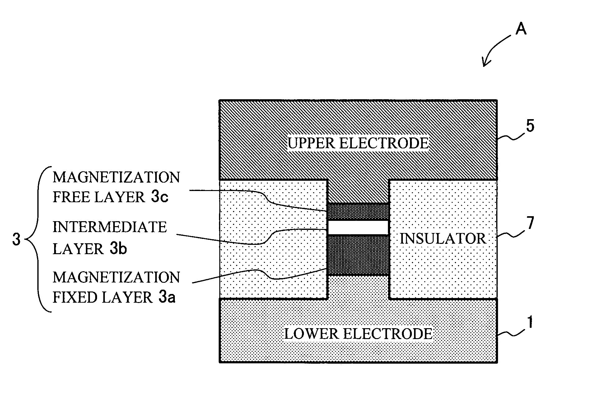
[0091]In the following, a microwave generating element and a microwave detecting element according to an embodiment of the invention are described. The present embodiment employs a ferromagnetic-multilayer-film magnetoresistance element having a structure such that current flows through a magnetization free layer / intermediate layer / magnetization fixed layer (the top-bottom positions of the magnetization free layer and the magnetization fixed layer may be reversed) formed on a substrate (such as, e.g., a columnar structure having a minute cross-sectional area perpendicular to the plane of the multilayer film). In the case of the microwave oscillating element, microwave is produced by magnetization resonance oscillation upon causing a flow of DC current. In the case of the microwave detecting element, DC voltage is produced by the detecting action of magnetization resonance oscillation upon irradiation of microwave.

[0092]First, an example of the structure of the magnetoresistance elem...

example 2

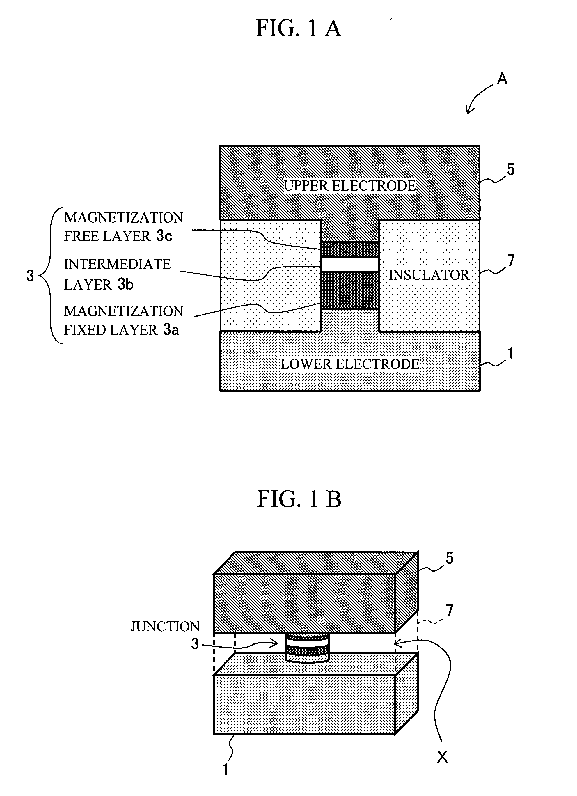
[0100]In the following, a magnetoresistance element used as a microwave generating element or a microwave detecting element according to the present embodiment is described with reference to the drawings. This embodiment adopts a structure (referred to as a point-contact configuration) in which the upper electrode (or lower electrode) alone is reduced in size, and the electrode is in contact with a multilayer film, of which the magnetoresistance element is formed, in a minute cross-sectional area. FIG. 3 is a cross section of an example of the magnetoresistance element of the present embodiment used for microwave generation or microwave detection. FIG. 4 is a perspective view of the magnetoresistance element. While FIGS. 3 and 4 show the example in which the upper electrode alone is reduced in size in point-contact configuration, it is also possible to adopt point-contact configuration on the lower electrode side. As shown in FIGS. 3 and 4, the magnetoresistance element A of the pre...

example 3

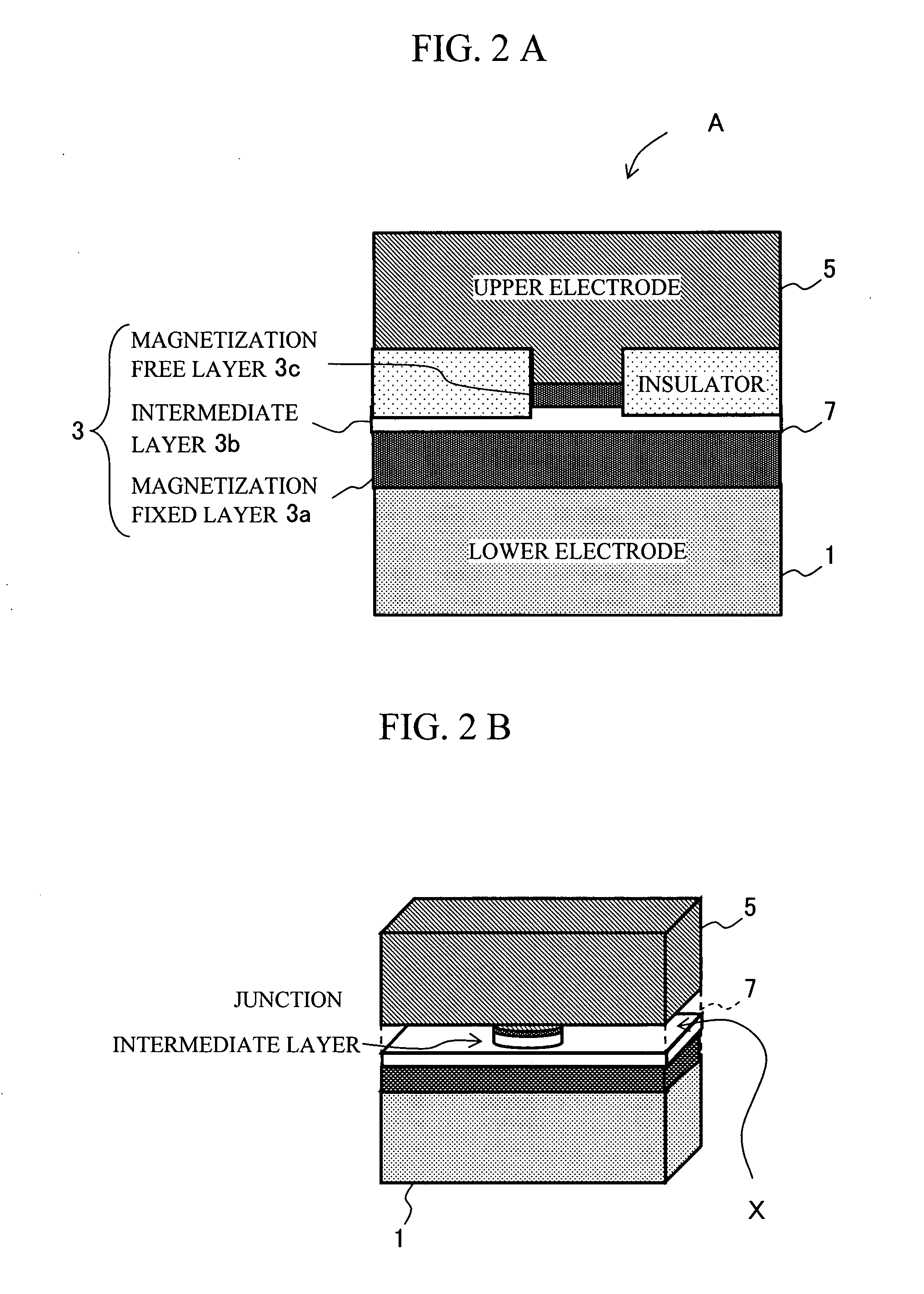
[0102]In the following, an example is described in which the above magnetoresistance element is used on the microwave transmission line. In the present embodiment, the magnetoresistance element is used as a microwave oscillation source (or detection element). In this case, the magnetoresistance element may be greatly smaller than a conventional microwave transmission circuit, and may be of a size smaller than 1 micron square, for example. Therefore, as shown in FIG. 5, by placing the magnetoresistance element A between a lower stripline 11 and an upper stripline 15, the element can be installed directly at the end of the microwave transmission line. In this case, the lower stripline 11 and the upper stripline 15 are electrically connected to each other via the magnetoresistance element alone. While in the example of FIG. 5 the magnetoresistance element is disposed on a coplanar-type stripline as the microwave transmission line, a slotline-type stripline may also be used. Preferably,...


PUM


Abstract

Microwave generating and detection portions of a electronic circuit is improved in efficiency and reduced in size. A microwave generating element A comprises a lower electrode 1, a layer 3 formed on the lower electrode 1 in an island shape, forming a magnetoresistance element, an insulator 7 formed on the lower electrode 1 in such a manner as to surround the layer 3 forming the magnetoresistance element, and an upper electrode 5 formed on the insulator 7 and the layer 3 forming the magnetoresistance element. The layer 3 forming the magnetoresistance element includes, in order from the side of the lower electrode 1, a magnetization fixed layer 3a, an intermediate layer 3b, and a magnetization free layer 3c. The magnetization free layer 3c, which is required to produce resonance oscillation based on a current, preferably is dimensioned to be equal to or smaller than 200 nm square in a cross-sectional area and on the order of 1 to 5 nm in film thickness, for example. The magnetization fixed layer 3a, when made of a single material, is required to have a thickness 10 times or more of the thickness of the magnetization free layer 3c. The magnetization fixed layer 3a may be comprised of a magnetic metal multilayer film that utilizes antiferromagnetic coupling.

Description

TECHNICAL FIELD[0001]The present invention relates to an element capable of generating a microwave and an element capable of detecting a microwave.BACKGROUND ART[0002]As operation speed of electronic devices become increasingly faster, an important issue is how to achieve higher integration (miniaturization) and higher efficiency in circuits handling microwaves (frequencies above the 1 GHz band). One typical example of a microwave oscillating source is the Gunn oscillator. The Gunn oscillator has the advantages of being able to operate at low voltages, and of having a high oscillation spectral purity (i.e., the percentage of frequency components outside the desired oscillation frequency is small). The Gunn oscillator, however, has the disadvantages of difficulty of size reduction for structural reasons and of poor oscillation efficiency (output power / input power=1% or less). For these reasons, it is now becoming more mainstream to use a method whereby an oscillation produced by a se...

Claims


Application Information

Patent Timeline
Patent Type & Authority Applications(United States)
IPC IPC(8): H03B15/00H01L43/08H01Q23/00
CPCH01L43/08H03B15/006H01Q23/00H01P11/003H10N50/10
Inventor SUZUKI, YOSHISHIGEYUASA, SHINJIFUKUSHIMA, AKIOTULAPURKAR, ASHWIN
Owner JAPAN SCI & TECH CORP
Why Eureka
Try Eureka