Semiconductor memory device and method of driving the same

Inactive Publication Date: 2008-06-26
ELPIDA MEMORY INC
View PDF2 Cites 14 Cited by
  • Summary
  • Abstract
  • Description
  • Claims
  • Application Information

AI Technical Summary

Benefits of technology

[0031]As described above, there are several problems with the overdrive technique in the related arts.
[0032]The external power supply direct coupling scheme has the problem that a sufficient operation margin for the sense amplifier cannot be maintained with respect to variations in the external power supply voltage. The internal power supply capacitive charge sharing scheme requires a large-capacitance capacitive element accompanying the internal power supply generation circuit which produces the overdrive voltage VOD. This is because capacitive charge sharing is performed and because there is a limit to the potential chargeable on the capacitance of bit lines and so on. The internal power supply capacitive charge sharing echeme also entails a problem that since the charge sharing voltage is fixed because of capacitive charge sharing, the VARY voltage potential cannot be changed as desired.
[0033]An exemplary object of the present invention is to provide an overdrive-type semiconductor memory device which uses an internal step-down power supply independent of an external power supply voltage, and which does not require an increased capacitance for overdrive voltage VOD.
[0034]Another exemplary object of the present invention is to provide an overdrive-type semiconductor memory device which uses an internal step-down power supply independent of an external power supply voltage, and which is capable of increasing array voltage VARY.
[0035]Still another exemplary object of the present invention is to provide a method of driving an overdrive-type semiconductor memory device which uses an internal step-down power supply independent of an external power supply voltage, which does not requir

Problems solved by technology

If the external power supply voltage varies, the boosting effect of the bit line BL by overdrive is changed and there is a possibility of the final potential on the bit line BL(H) becoming excessively higher or excessively lower than the array voltage VARY.
That is, the external power supply voltage VDD varies, a problem arises that the operation margin of the sense amplifier is considerably reduced.
This problem becomes more serious with reduction in voltage, for example, when the external power supply voltage is reduced to 1 V.
In this case, the load drive capacity of the on-chip power supply circuit for generating the overdrive voltage VOD is insufficient for the load capacitance.
Therefore the VARY potential cannot be increased.
If the VARY potential is increased by newly setting the capacitance value of capacitive element 20, the necessary capacitance of capacitive element 20 becomes much higher, which is considerably disadvantageous from the viewpoint of an area condition for the DRAM.
Thus, with overdrive by the internal power supply capacitive charge sharing scheme, there is a prob

Method used


Image

  • Semiconductor memory device and method of driving the same
  • Semiconductor memory device and method of driving the same
  • Semiconductor memory device and method of driving the same

Examples


Embodiment Construction

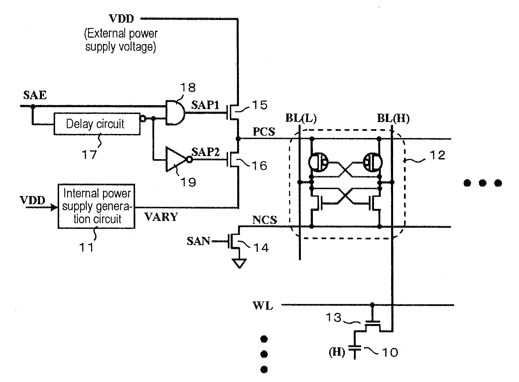
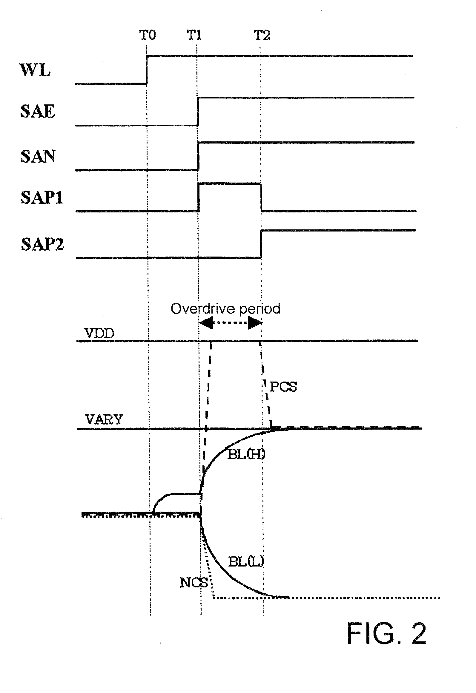
[0049]FIG. 5 shows an example of an array circuit using an overdrive in a semiconductor memory device according to an exemplary embodiment of the present invention. Description will be made by assuming that the semiconductor memory device is a DRAM. The circuit shown in FIG. 5 is similar to the circuit shown in FIG. 3, in which overdrive according to the internal power supply capacitive charge sharing scheme is executed, but differs from the circuit shown in FIG. 3 in operation timing in internal power supply generation circuit 21 for generating overdrive voltage VOD as an internal stepped-down voltage from external power supply voltage VDD, and also differs from the circuit shown in FIG. 3 in that delay circuit 31 is capable of changing the delay time. FIG. 6 shows operating waveforms in the circuit shown in FIG. 5.

[0050]Since the semiconductor memory device in the present exemplary embodiment is a DRAM, memory cell 10 is a dynamic-type memory cell. In the circuit shown in FIG. 5, ...


PUM


Abstract

A semiconductor memory device includes a first circuit which generates a first potential lower than the external power supply voltage, a second circuit which generates a second potential lower than the first potential, a capacitor charged to the first potential, a bit line connected to a memory cell, a sense amplifier which performs sense operation to amplify a potential on the bit line to the second potential, and a connection control circuit which connects the first circuit to the sense amplifier within a first time period from a start of the sense operation, and which connects the second circuit to the sense amplifier after the lapse of the first time period. The first circuit is enabled before the start of the sense operation and is disabled after the completion of charging of the capacitor, and the output of the first circuit is thereby set in a floating state.

Description

[0001]This application is based upon and claims the benefit of priority from Japanese patent application No. 2006-348112, filed on Dec. 25, 2006, the disclosure of which is incorporated herein in its entirety by referenceBACKGROUND OF THE INVENTION[0002]1. Field of the Invention[0003]The present invention relates to a semiconductor memory device and a method of driving the semiconductor memory device. More particularly, the present invention relates to a semiconductor memory device which has a memory cell array and sense amplifiers operating on an internal stepped-down voltage generated from an external power supply voltage, and for which a charge-sharing overdrive scheme to accelerate sensing speed is used, and to a method of driving such a semiconductor memory device.[0004]2. Description of the Related Art[0005]In general, in a semiconductor memory device to which an external power supply voltage is supplied from the outside, an internal stepped-down voltage having an absolute val...

Claims


Application Information

Patent Timeline
IPC IPC(8): G11C5/14
CPCG11C5/147G11C7/065G11C2207/065G11C11/4074G11C11/4091G11C7/08
Inventor OHATA, MUNETOSHITERAMOTO, KAZUHIROMOCHIDA, NORIAKI
Owner ELPIDA MEMORY INC
Why Eureka
Try Eureka