Semiconductor device and timing control method for the same

a technology of electromagnetic field and timing control method, which is applied in the direction of pulse technique, digital storage, instruments, etc., can solve the problems of difficulty in achieving a sufficient operating margin, and achieve the effect of sufficient operating margin, sufficient operating margin, and reduced current consumption

Active Publication Date: 2009-04-30
LONGITUDE SEMICON S A R L
View PDF13 Cites 1 Cited by
  • Summary
  • Abstract
  • Description
  • Claims
  • Application Information

AI Technical Summary

Benefits of technology

[0011]According to the embodiment, a source transistor serving as the power supply control portion is turned ON in response to the rising of clock, and then a command signal as the input signal is supplied to the internal circuit in response to the falling of the clock. This assures a sufficient operating margin, and enables the semiconductor device to operate at an even higher speed. Further, the embodiment, which assures the sufficient operating margin, eliminates the need of turning the power supply control portion ON in a previous cycle. Accordingly, the current consumption can be reduced.

Problems solved by technology

The present inventors have recognized that the increased operation speed is a cause of difficulty in achieving a sufficient operating margin.

Method used


Image

  • Semiconductor device and timing control method for the same
  • Semiconductor device and timing control method for the same
  • Semiconductor device and timing control method for the same

Examples


first embodiment

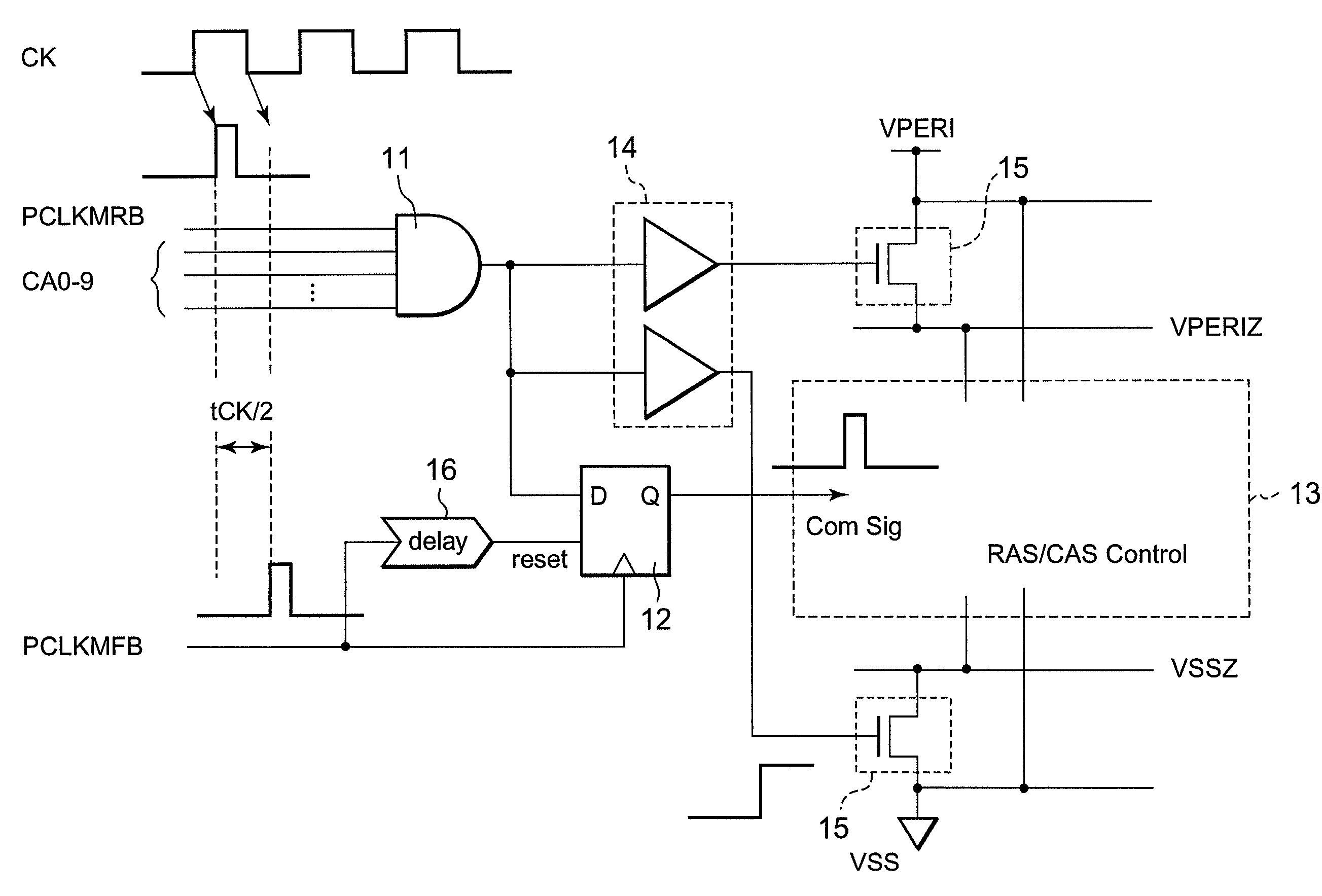
[0027]FIG. 3 is a block diagram showing a memory control unit and source transistor control unit of a semiconductor device according to the present invention.

[0028]The memory control unit has a command decode portion (command decoder) 11, a fall command latch portion (fall command latch) 12, and a memory operation control portion (RAS / CAS control) 13.

[0029]The source transistor control unit has a driver portion (Source Tr. Driver) 14 and a source transistor portion (Source Tr) 15.

[0030]The command decode portion 11 operates as input means (or an input portion) for the memory operation control portion 13. Specifically, the command decode portion 11 decodes a memory operation control command input to command pins CA0 TO CA9 and outputs an internal command signal in synchronization with a first clock PCLKMRB.

[0031]The fall command latch portion (D latch) 12 latches the internal command signal received from the command decode portion 11 in synchronization with a second clock PCLKMFB and...

second embodiment

[0045]A semiconductor device according to the present invention will be described in detail with reference to FIG. 5.

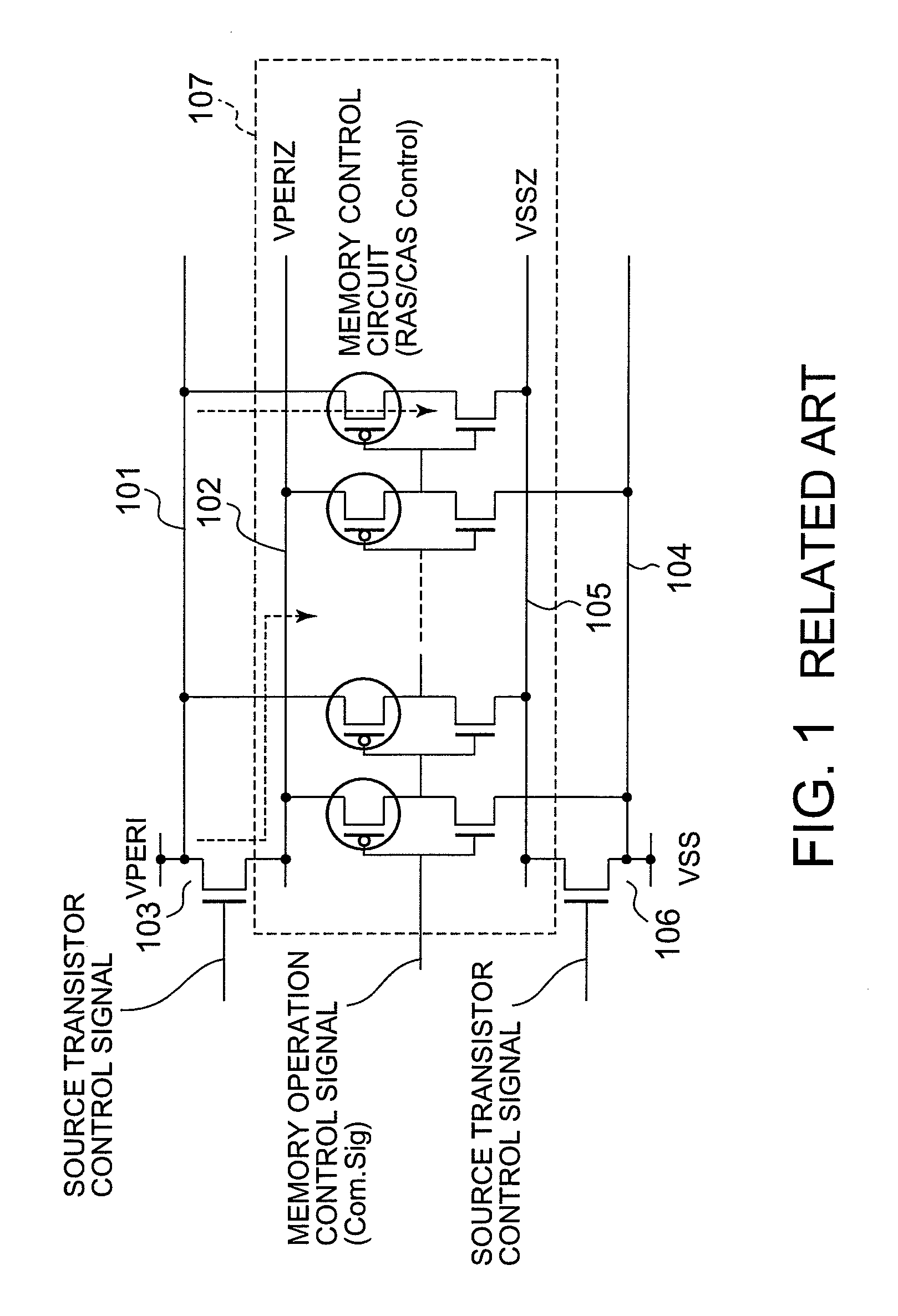
[0046]FIG. 5 is a block diagram showing a memory control unit and a source transistor control unit of the semiconductor device according to the second embodiment of the present invention. In FIG. 5, like components to those of FIG. 1 are given like reference characters.

[0047]In this second embodiment, a single source transistor driver 21 is provided in place of the driver portion 14 of the first embodiment. The circuit configuration can be simplified by using this single source transistor driver 21 to turn ON and OFF the pair of the source transistors of the source transistor portion 15.

[0048]In the second embodiment, a fall command decode portion 22 formed with a logic circuit as latch means is provided in place of the fall command latch portion 12. Alternatively, a through latch may be used as the latch means.

[0049]According to the second embodiment, like the first ...


PUM


Abstract

A semiconductor device includes a power-supply control portion and a latch portion. The power-supply control portion supplies power to an internal circuit in response to an input signal synchronized with rising of clock. The latch portion latches the input signal in synchronization with falling of the clock and supplies the latched input signal to the internal circuit.

Description

[0001]This application is based upon and claims the benefit of priority from Japanese Patent Application No. 2007-279520, filed on Oct. 26, 2007, the disclosure of which is incorporated herein in its entirety by reference.BACKGROUND OF THE INVENTION [0002]The present invention relates to a semiconductor device and a timing control method for the same, and in particular to a semiconductor device including an internal circuit connected to a power supply via a source transistor as well as to a timing control method for such a semiconductor device.[0003]The recent development of semiconductor memories has decreased the operating voltage while having increased the operating frequency. In LPDDR2-SDRAMs (Low Power Double Data Rate2 Synchronous Dynamic Random Access Memories) (hereafter, referred to simply as LPDDR2), for example, the power supply voltage of a peripheral circuit is 1.2V and the operating frequency is 667 MHz.[0004]In order to realize rapid operation, the Vt (threshold volta...

Claims


Application Information

Patent Timeline
Patent Type & Authority Applications(United States)
IPC IPC(8): H03K3/356
CPCG11C11/4074G11C11/4076H03K3/356113H03K3/012G11C2207/2227
Inventor YOKO, HIDEYUKITAKISHITA, RYUUJI
Owner LONGITUDE SEMICON S A R L
Why Eureka
Try Eureka