Shifter register for low power consumption application

a shift register and low power consumption technology, applied in the field of shift register circuits, can solve the problems that the shift register using the stage circuit of fig. 1 can consume a significant amount of power, and the power consumption in these clock buffers is equal, so as to reduce power consumption, improve speed, and reduce signal resistance

a shift register and low power consumption technology, applied in the field of shift register circuits, can solve the problems that the shift register using the stage circuit of fig. 1 can consume a significant amount of power, and the power consumption in these clock buffers is equal, so as to reduce power consumption, improve speed, and reduce signal resistance

US20080152072A1Active Publication Date: 2008-06-26KOPIN CORPORATION

Image

  • Shifter register for low power consumption application
  • Shifter register for low power consumption application
  • Shifter register for low power consumption application

Examples


Embodiment Construction

[0022]A description of example embodiments of the invention follows.

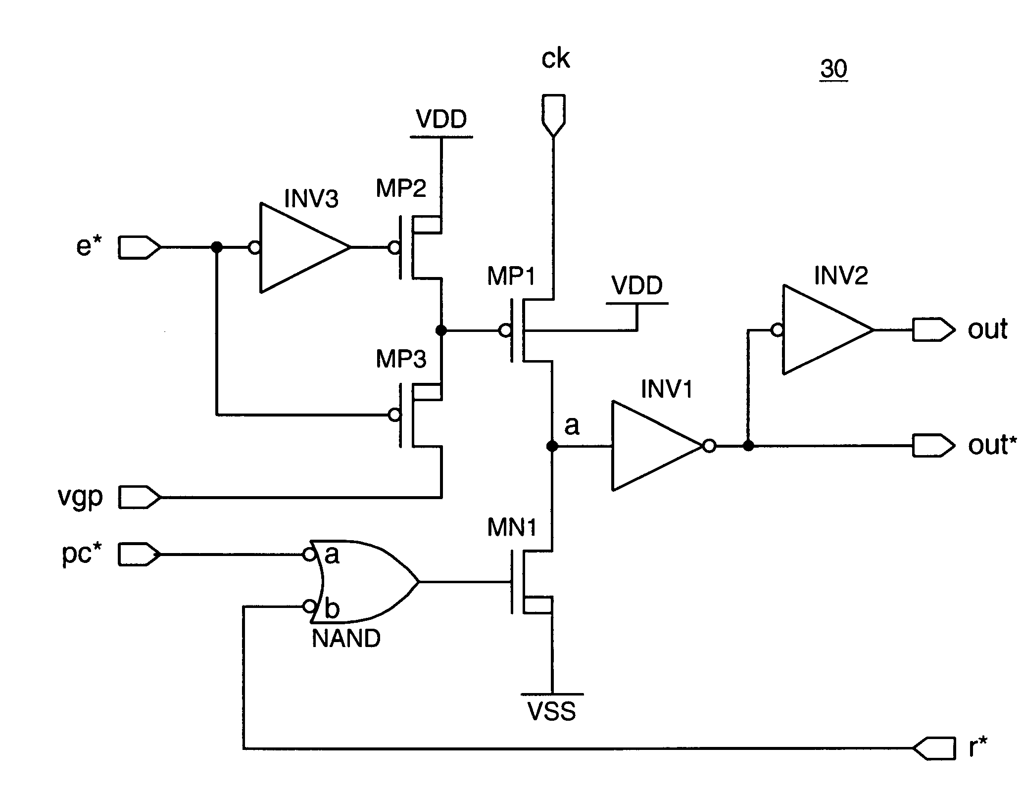
[0023]FIG. 3 illustrates a circuit 30 that improves over the arrangements of FIGS. 1 and 2. Here, the clock signal input ck also drives a stage transistor MP1. However, the gate of MP1 is fed from a pair of cascode transistors MP2 and MP3 that set the state at node a as determined by inputs e* and vgp. The inverted input from the previous stage e* is fed to the input terminal of inverter INV3 to control the gate of transistor MP3. The MP3 drain terminal controls the gate of transistor MP1. The source terminal of transistor MP2 is fed from voltage VDD.

[0024]An intended pre-charge input pc* is fed through the single NAND gate together with a reset signal r*. The output of the single NAND gate drives the gate terminal of signal buffer transistor MN1. The first inverter INV1 and second inverter INV2 provide, respectively, the inverted outputs out* and non-inverted output out.

[0025]Operation of circuit 20 is similar to t...


PUM


Abstract

A high voltage shift register stage which directly accepts low voltage clock signal inputs without using clock buffers. In particular, a shift register stage circuit is adapted to operate with a low voltage swing clock signal, with the stage circuit having a single state node, a, driven directly. This arrangement allows for reduced power consumption and higher operating speeds.

Description

RELATED APPLICATION(S)[0001]This application claims the benefit of U.S. Provisional Application No. 60 / 860,059, filed on Nov. 20, 2006. The entire teachings of the above application(s) are incorporated herein by reference.BACKGROUND OF THE INVENTION[0002]The present invention relates to shift register circuits, and more particularly to shift register designs adapted for providing the lowest possible power consumption.[0003]FIG. 1 illustrates one conventional design for a single stage static shift register. As with any shift register, this circuit 10 has a signal input in, a clock ck and in this configuration complimentary outputs out and out *. The circuit is powered by a supply voltage provided by two rail voltages VDD and VSS.[0004]This specific circuit uses an input signal buffer transistor MP1 that feeds a pair of cross-coupled transistors MP2 and MP3 to store the input signal state. Inverters INV1 and INV2 connected to the output of MP1 serve to buffer output voltage and curren...

Claims


Application Information

Patent Timeline
26 Jun 2008
Publication
US20080152072A1
IPC
G11C19/00
CPC
G11C19/28
Inventors
HERRMANN, FREDERICK P.; ZHANG, KUN