Stress liner surrounded facetless embedded stressor mosfet

a stress liner and embedded stressor technology, applied in the field of metal oxide semiconductor field effect transistors (mosfets), can solve the problems of reducing the benefit of embedded stressors, and achieve the effect of improving performan

Inactive Publication Date: 2008-07-03
GLOBALFOUNDRIES INC
View PDF5 Cites 51 Cited by
  • Summary
  • Abstract
  • Description
  • Claims
  • Application Information

AI Technical Summary

Benefits of technology

[0005]The present invention provides an STI bounded transistor structure having enhanced performance which is not diminished due t

Problems solved by technology

However, due to the epitaxial process nature of forming such stressors, the edge of shallow trench isolat

Method used


Image

  • Stress liner surrounded facetless embedded stressor mosfet
  • Stress liner surrounded facetless embedded stressor mosfet
  • Stress liner surrounded facetless embedded stressor mosfet

Examples


Embodiment Construction

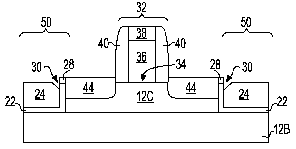
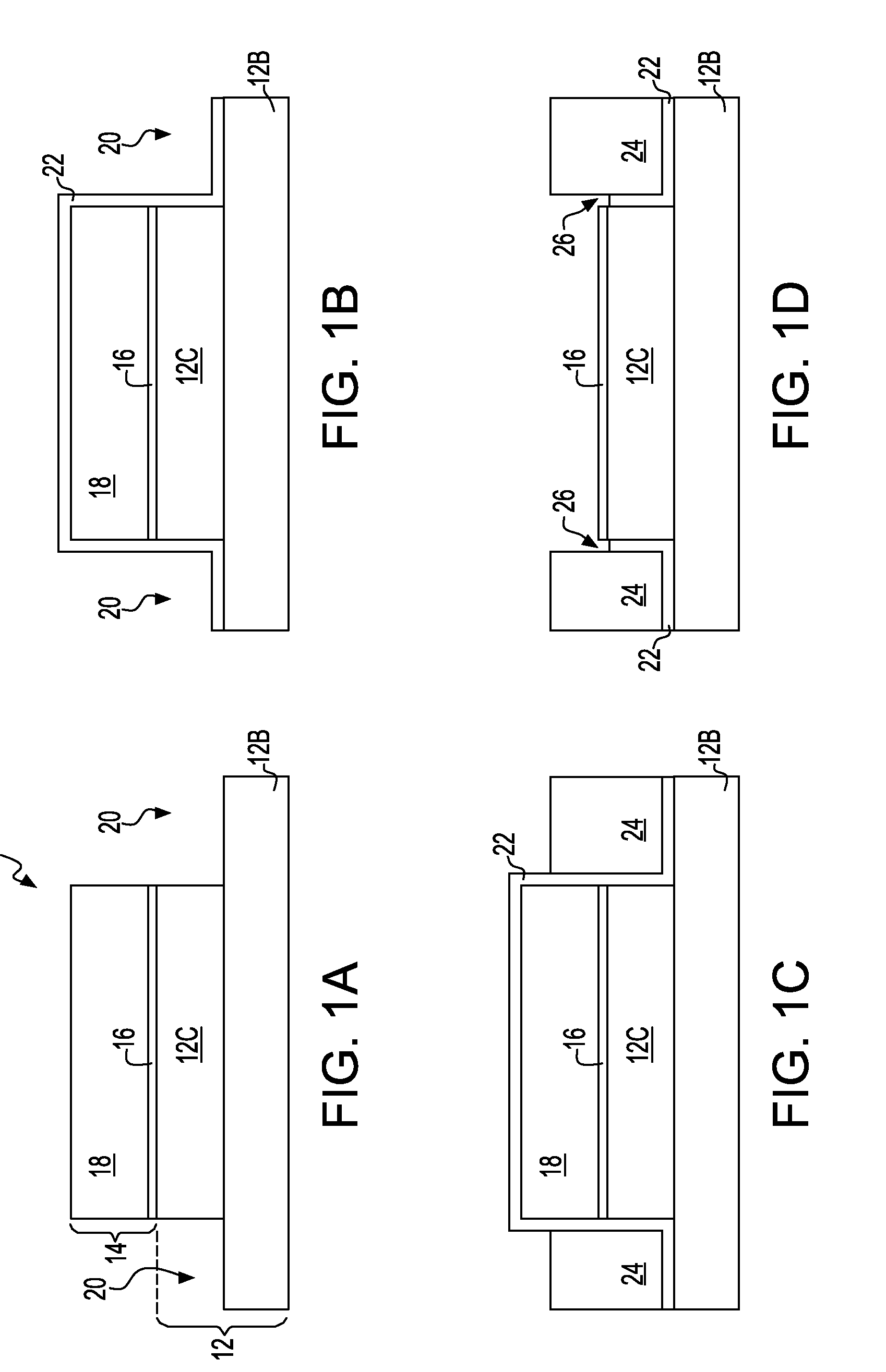
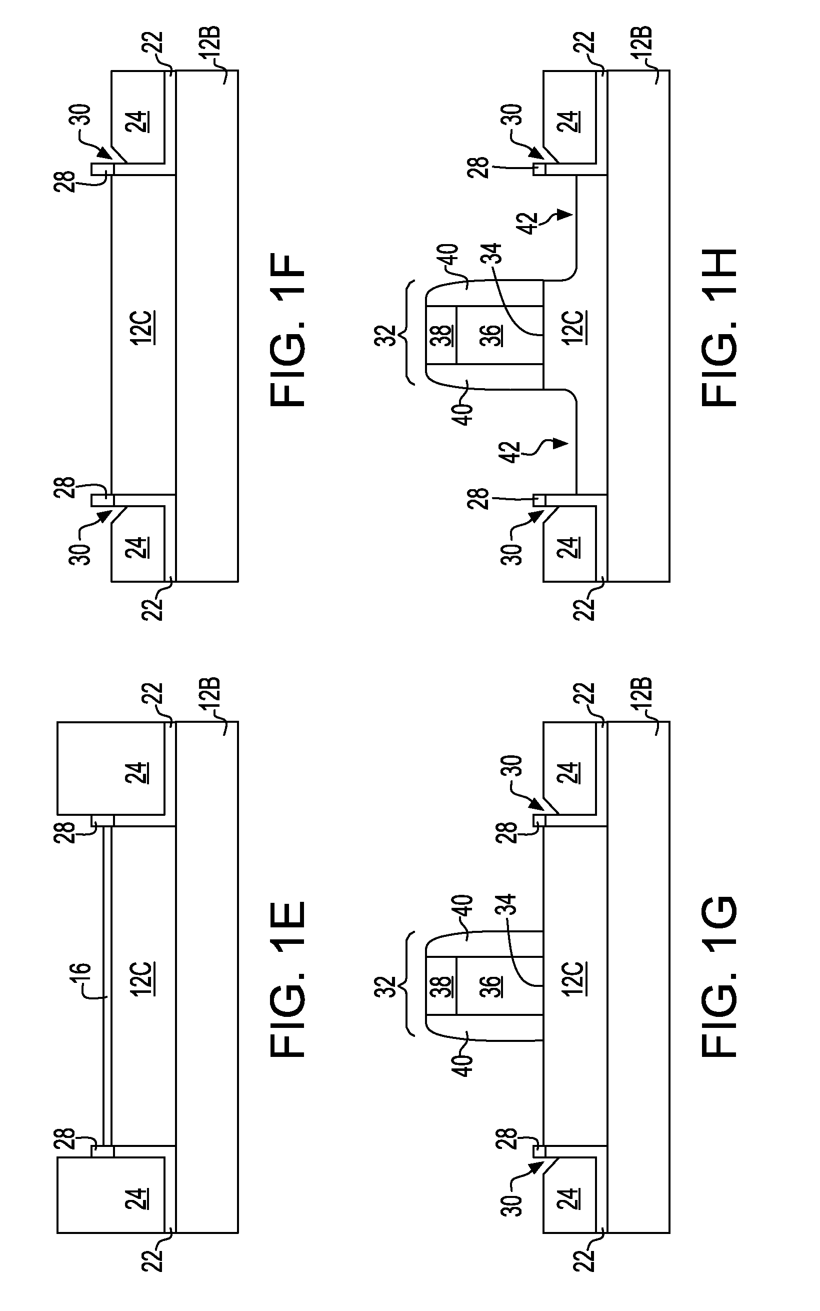
[0019]The present invention, which provides a stress liner surrounded facetless embedded stressor MOSFET and a method of fabricating the same, will now be described in greater detail by referring to the following description and drawings that accompany the present application. It is noted that the drawings of the present application are provided for illustrative purposes and, as such, they are not drawn to scale.

[0020]In the following description, numerous specific details are set forth, such as particular structures, components, materials, dimensions, processing steps and techniques, in order to provide a thorough understanding of the present invention However, it will be appreciated by one of ordinary skill in the art that the invention may be practiced without these specific details. In other instances, well-known structures or processing steps have not been described in detail in order to avoid obscuring the invention.

[0021]It will be understood that when an element as a layer, ...


PUM


Abstract

The present invention provides an STI bounded transistor structure having enhanced performance which is not diminished due to embedded stressor facets that can be present at the edge of the source/drain regions that contacts an embedded stressor material. Considering that the facet in the prior art is due to an STI divot formed during several necessary wet etching processes, the MOSFET source/drain edge of the inventive structure is surrounded by a liner to prevent facet growth during the epitaxial growth of the stressor material. As such, a part of the semiconductor substrate edge is preserved. The liner employed in the present invention is a stress engineering material such as, for example, silicon nitride.

Description

FIELD OF THE INVENTION [0001]The present invention relates to a semiconductor structure, and more particularly to a metal oxide semiconductor field effect transistor (MOSFET) having enhanced performance.BACKGROUND OF THE INVENTION [0002]Mechanical stresses within a semiconductor device substrate have been widely used to modulate and / or boast device performance. For example, in common Si technology, the channel of a transistor is oriented along the <110> direction on {100} planes of silicon. In this arrangement, hole mobility is enhanced when the channel is under compressive stress in the current flow direction and / or under tensile stress in a directional normal of the channel, while electron mobility is enhanced when the channel is under tensile stress in both parallel and normal direction of channel. Therefore, compressive and / or tensile stresses can be advantageously created in the channel regions of a p-channel field effect transistor (pFET) and / or an n-channel field effect...

Claims


Application Information

Patent Timeline
IPC IPC(8): H01L29/78
CPCH01L29/165H01L29/201H01L29/221H01L29/66628H01L29/78684H01L29/66772H01L29/78H01L29/7846H01L29/7848H01L29/66636
Inventor KIM, BYEONG Y.BUTT, SHAHID A.CHEN, XIAOMENGJENG, SHWU-JEN J.NAYFEH, HASAN M.WEHELLA-GAMAGE, DEEPAL
Owner GLOBALFOUNDRIES INC
Why Eureka
Try Eureka