Tunable gate electrode work function material for transistor applications

a work function and transistor technology, applied in the field of transistor gate electrode materials, can solve the problems of inability to achieve ideal threshold voltages for inability to use n-type and p-type metal gate materials used to set work functions, and inability to achieve ideal threshold voltages for both pmos (a mosfet with a p-channel) and nmos

Active Publication Date: 2008-07-03
TAHOE RES LTD
View PDF7 Cites 182 Cited by
  • Summary
  • Abstract
  • Description
  • Claims
  • Application Information

AI Technical Summary

Problems solved by technology

A “mid-gap” work function gate electrode that is located too close to the middle of the p and n channel work function range is inadequate because it typically results in a transistor having either a threshold voltage that is too large for high-performance applications or a compromised SCE when the effective channel doping is reduced to lower the threshold voltage.
Therefore, a single mid-gap gate material is also incapable of achieving ideal threshold voltages for both pMOS (a MOSFET with a p-channel) and nMOS (a MOSFET with an n-channel) multi-gate transistors.
The n-type and p-type metal gate materials used to set work function may not be good conductors.
However, even with silicided polysilicon cap 180, the bulk resistance of the gate electrode, becomes unacceptably high as the dimension of the gate electrode is scaled.
While a low resistance metal, such as aluminum, could be employed to further lower the gate electrode bulk resistance below that achievable with silicided polysilicon cap 180, the presence of a low resistance capping metal in close proximately to the MOS junction is problematic for many reasons.
Most notably, diffusion of the capping metal into the MOS junction can cause deep level traps shifting threshold voltages or otherwise render a transistor inoperable.

Method used


Image

  • Tunable gate electrode work function material for transistor applications
  • Tunable gate electrode work function material for transistor applications
  • Tunable gate electrode work function material for transistor applications

Examples


Embodiment Construction

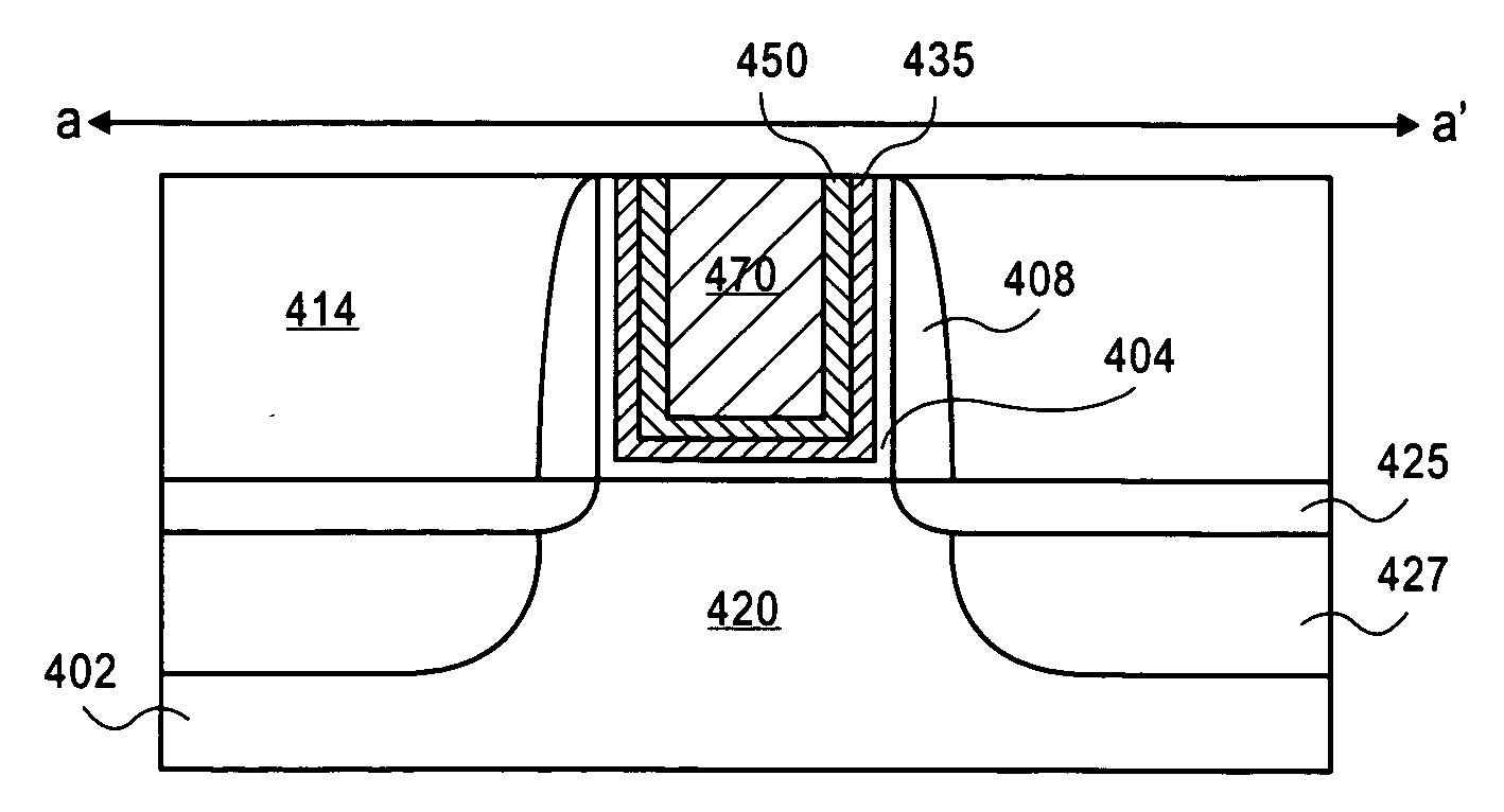
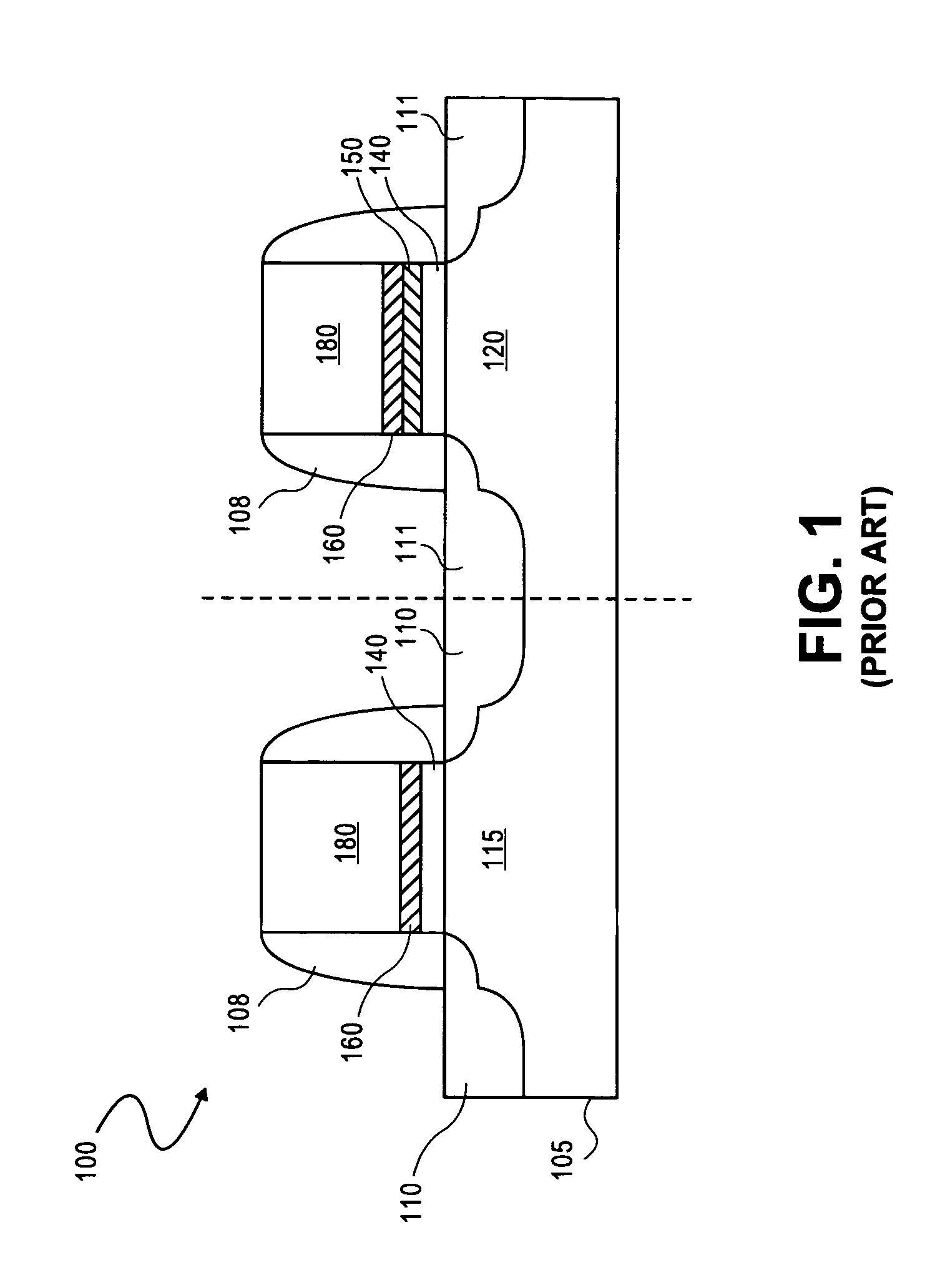
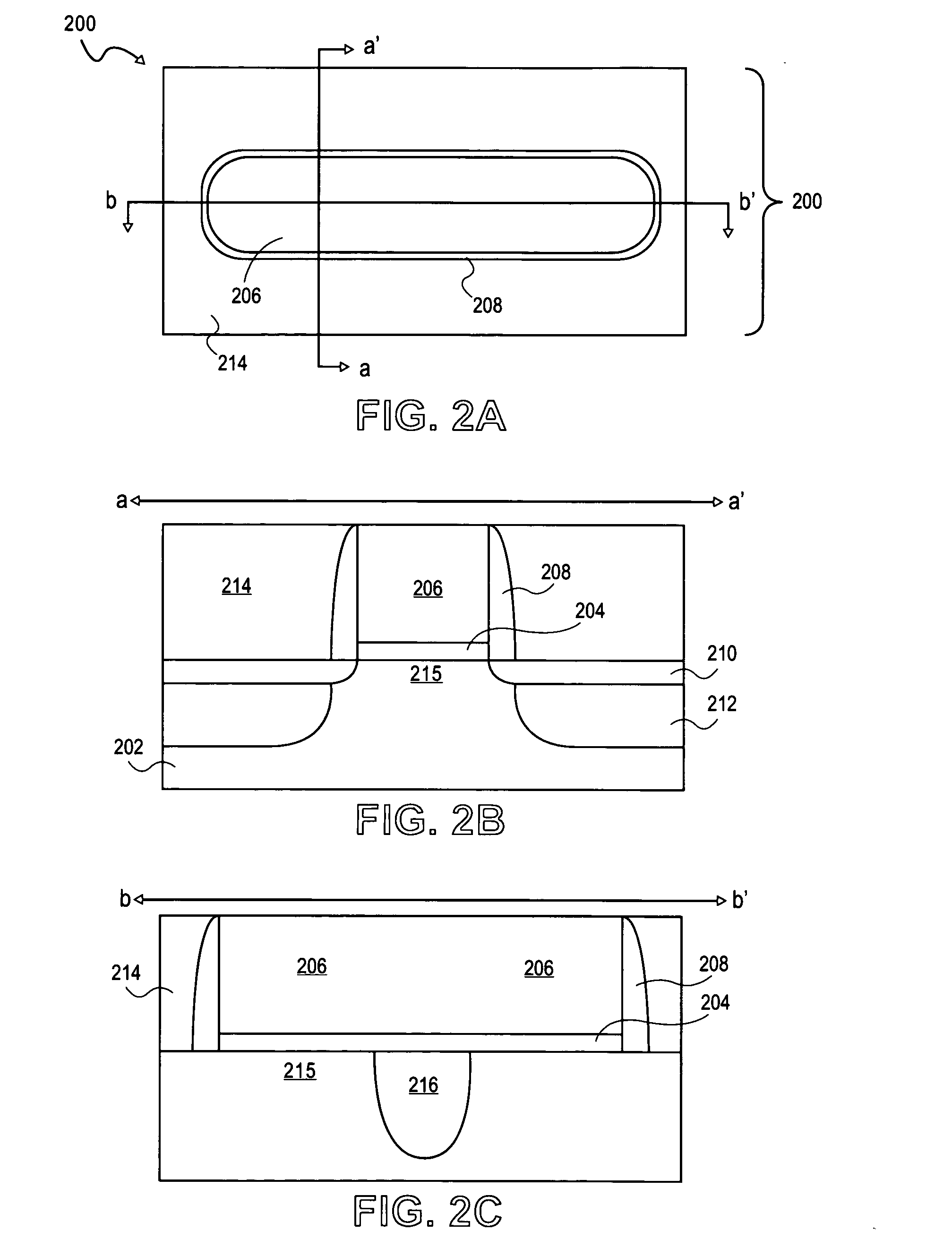
[0013]In various embodiments, a gate metal stack for CMOS is described with reference to figures. However, certain embodiments may be practiced without one or more of these specific details, or in combination with other known methods and materials. In the following description, numerous specific details are set forth, such as specific materials, dimensions and processes, etc., in order to provide a thorough understanding of the present invention. In other instances, well-known semiconductor processes and manufacturing techniques have not been described in particular detail in order to not unnecessarily obscure the present invention. Reference throughout this specification to “an embodiment” means that a particular feature, structure, material, or characteristic described in connection with the embodiment is included in at least one embodiment of the invention. Thus, the appearances of the phrase “in an embodiment” in various places throughout this specification are not necessarily r...


PUM

PropertyMeasurementUnit
work functionaaaaaaaaaa
temperatureaaaaaaaaaa

Abstract

Described herein are metal gate electrode stacks including a low resistance metal cap in contact with a metal carbonitride diffusion barrier layer, wherein the metal carbonitride diffusion barrier layer is tuned to a particular work function to also serve as a work function metal for a pMOS transistor. In an embodiment, the work function-tuned metal carbonitride diffusion barrier prohibits a low resistance metal cap layer of the gate electrode stack from migrating into the MOS junction. In a further embodiment of the present invention, the work function of the metal carbonitride barrier film is modulated to be p-type with a pre-selected work function by altering a nitrogen concentration in the film.

Description

BACKGROUND OF THE INVENTION[0001]1. Field of the Invention[0002]The present invention relates to semiconductor device manufacture. More particularly this invention relates to transistor gate electrode materials.[0003]2. Discussion of Related Art[0004]During the past two decades, the physical dimensions of MOSFETs have been aggressively scaled for low-power, high-performance CMOS applications. In order to continue scaling future generations of CMOS, the use of metal gate electrode technology is important. For example, further gate insulator scaling will require the use of dielectric materials with a higher dielectric constant than silicon dioxide. Devices utilizing such gate insulator materials demonstrate vastly better performance when paired with metal gate electrodes rather than traditional poly-silicon gate electrodes.[0005]Depending on the design of the transistors used in the CMOS process, the constraints placed on the metal gate material are somewhat different. For a planar, b...

Claims


Application Information

Patent Timeline
Patent Type & Authority Applications(United States)
IPC IPC(8): H01L27/092H01L21/8238H01L21/28
CPCH01L21/823842H01L29/7833H01L29/4966H01L29/4958
Inventor LAVOIE, ADRIEN R.DUBIN, VALERY M.PLOMBON, JOHN J.DOMINGUEZ, JUAN E.SIMKA, HARSONO S.HAN, JOSEPH H.DOCZY, MARK
Owner TAHOE RES LTD
Why Eureka
Try Eureka