Package on package structure for semiconductor devices and method of the same

Inactive Publication Date: 2008-07-03
ADVANCED CHIP ENG TECH
View PDF7 Cites 60 Cited by
  • Summary
  • Abstract
  • Description
  • Claims
  • Application Information

AI Technical Summary

Benefits of technology

[0010]An object of the present invention is to provide a semiconductor device package (chip assembly) wi

Problems solved by technology

Such packages work well to protect IC dice, but they can be more bulky than desirable for certain multi-chip applications requiring compact die packaging.
As a semiconductor become more complicated, the traditional package technique, for example lead frame package, flex package, rigid package technique, can't meet the demand of producing smaller chip with high density elements on the chip.
Typical BGA packages include a convoluted signal path, giving rise to high impedance and an inefficient thermal path which results in poor thermal dissipation performance.
Recently, integrated circuit (chip) pack

Method used


Image

  • Package on package structure for semiconductor devices and method of the same
  • Package on package structure for semiconductor devices and method of the same
  • Package on package structure for semiconductor devices and method of the same

Examples


Embodiment Construction

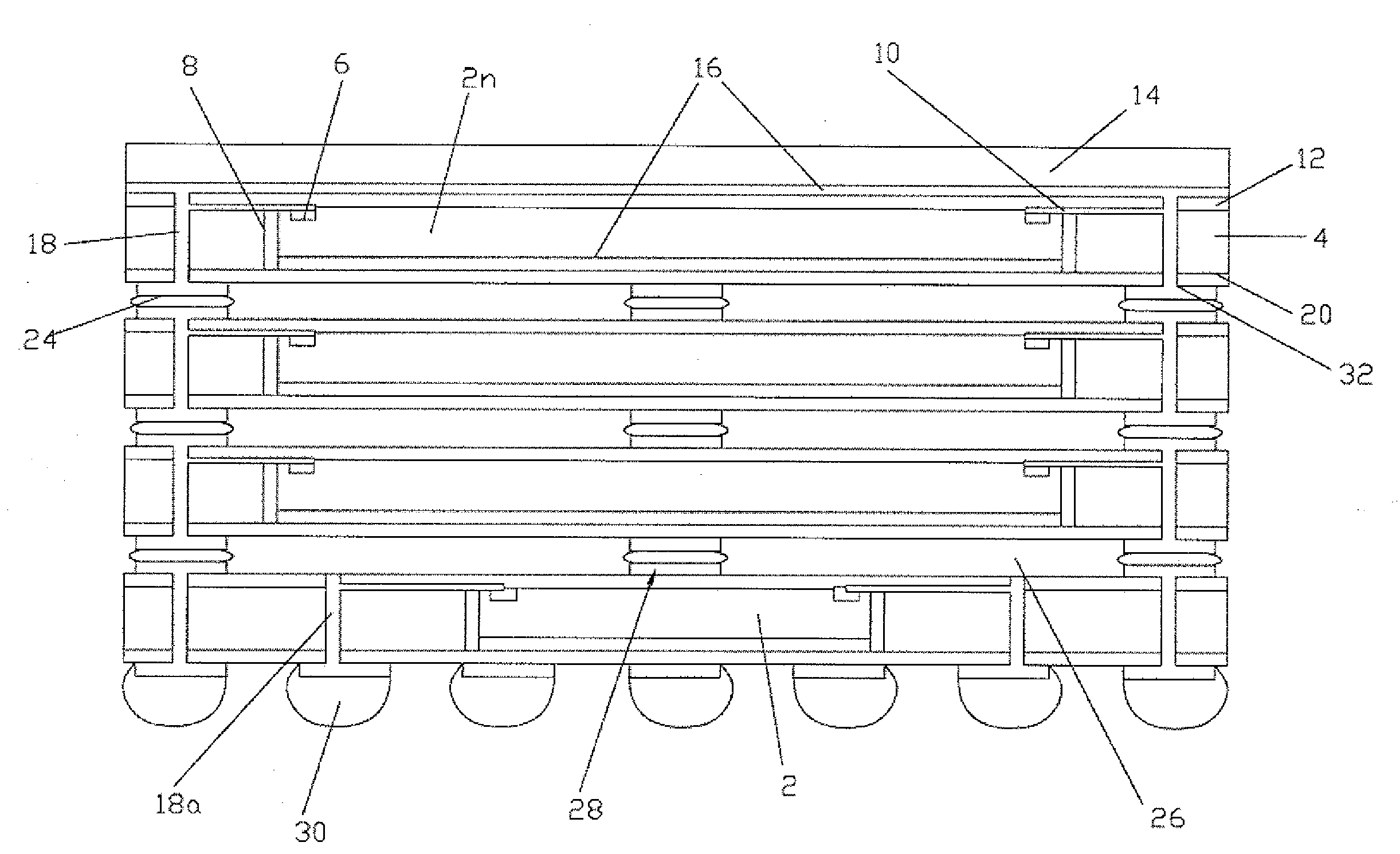
[0021]The invention will now be described in greater detail with preferred embodiments of the invention and illustrations attached. Nevertheless, it should be recognized that the preferred embodiments of the invention is only for illustrating. Besides the preferred embodiment mentioned here, present invention can be practiced in a wide range of other embodiments besides those explicitly described, and the scope of the present invention is expressly not limited expect as specified in the accompanying claims.

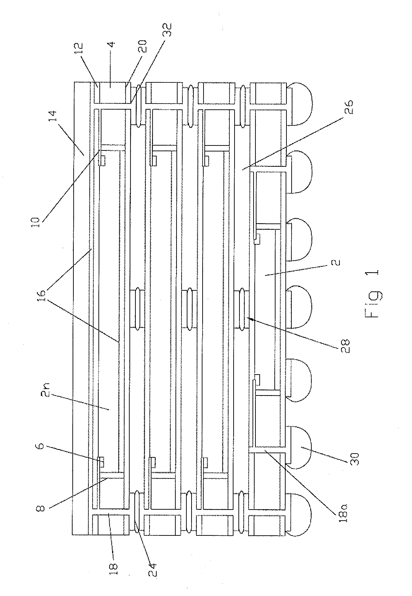
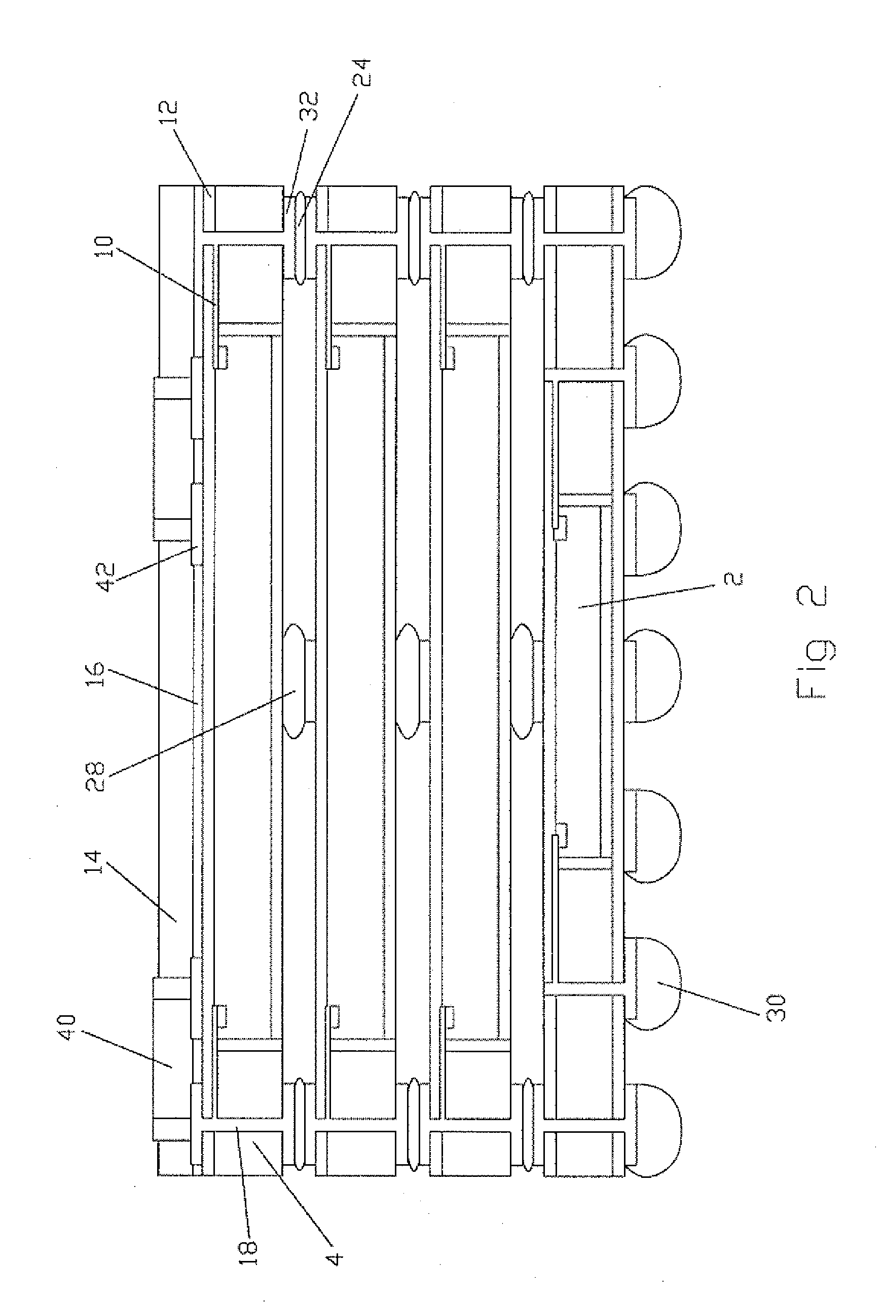
[0022]The present invention discloses a semiconductor device multi-package structure. The present invention provide a semiconductor chip assembly which includes chip, conductive trace and metal inter-connecting as shown in FIGS. 1-5. The major components and the structure of each individual package are almost identical. The embodiment will be described by using the most upper package for illustration.

[0023]The individual package includes a chip 2n which is surrounded by core mater...


PUM


Abstract

A package on package structure for semiconductor devices comprises at least one first level package having at least first level semiconductor die therein, wherein the package having first level contact pads formed on a first upper and lower surfaces of the first level package, the first level package having a first level upper build up layers and/or a first level lower build up layer to couple to bonding pads of the first level semiconductor die to contact first level pads on the both upper and lower surfaces of the first level package; a second level package having at least one second semiconductor die contained therein, wherein the second level package has a second level contact pads on a second upper and lower surfaces of the second level package, and conductive connecting through holes; wherein the second level package have a second level upper build up layer and/or second level lower build up layer to couple second level bonding pads of the second semiconductor die to contact second level pads and the conductive connecting through holes on the upper and lower surface of the second level package, conductive through holes being coupled to the first level pads of upper and lower surfaces of the first level package and the second level pads of upper and lower surface of the second level package; and adhesion materials attached on lower surface of the first level package and the upper surface of the second level package.

Description

RELATED APPLICATIONS[0001]The present application is a continuation-in-part (CIP) application of a pending U.S. application, Ser. No. 11 / 648,688, entitled “Wafer Level Package with Die Receiving Through-Hole and Method of the Same”, and filed on Jan. 3, 2007, and a pending U.S. application Ser. No. 11 / 694,719, entitled “Semiconductor Device Package with Die Receiving Through-hole and Dual Build-up Layers over Both Side-surfaces for WLP and Method of the Same”, and filed on Mar. 30, 2007, said applications incorporated herein by reference in their entirety.BACKGROUND OF THE INVENTION[0002]1. Field of Invention[0003]This invention relates to a semiconductor package, and more particularly to package on package for semiconductor devices.[0004]2. Description of the Prior Art[0005]Integrated circuit (IC) dice or “chips” are small, generally rectangular IC devices cut from a semiconductor wafer, such as a silicon wafer, on which multiple ICs have been fabricated. Traditionally, bare IC dic...

Claims


Application Information

Patent Timeline
IPC IPC(8): H01L23/02H01L21/00
CPCH01L25/105H01L2924/3011H01L2224/73267H01L2225/1058H01L24/19H01L2225/1035H01L2924/14H01L2924/00
Inventor YANG, WEN-KUN
Owner ADVANCED CHIP ENG TECH
Why Eureka
Try Eureka