Semiconductor device

Active Publication Date: 2008-07-10
MAXPOWER SEMICON INC
View PDF32 Cites 104 Cited by
  • Summary
  • Abstract
  • Description
  • Claims
  • Application Information

AI Technical Summary

Benefits of technology

[0028]Numerous benefits are achieved using the present invention over conventional techniques. For example, in an embodiment according to the present invention, improved MOSFET conduction and switching performance is achieved. Moreover, in other embodiments, paralleling of alternate charge balanced dielectric and silicon layers provides a device with performance exceeding the one dimensional silicon breakdown voltage limit for a given doping concentration. The use of fixed charge reduces the capacitances compared to conventional techniqu

Problems solved by technology

In a SJ structure, the minimum widths of the n-type and p-type pillars set a limitation on reducing cell pitch and scaling the device.
There are also several

Method used


Image

  • Semiconductor device
  • Semiconductor device
  • Semiconductor device

Examples


Embodiment Construction

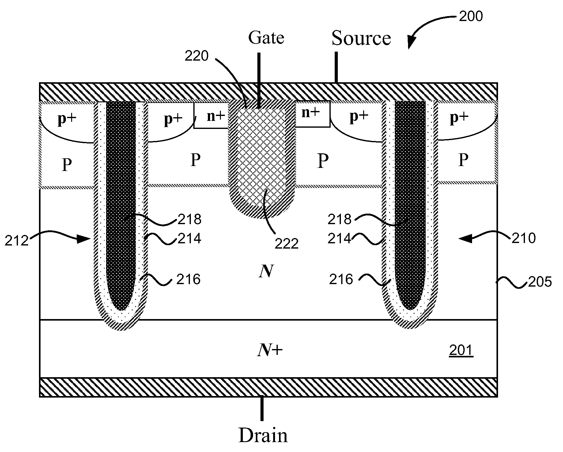
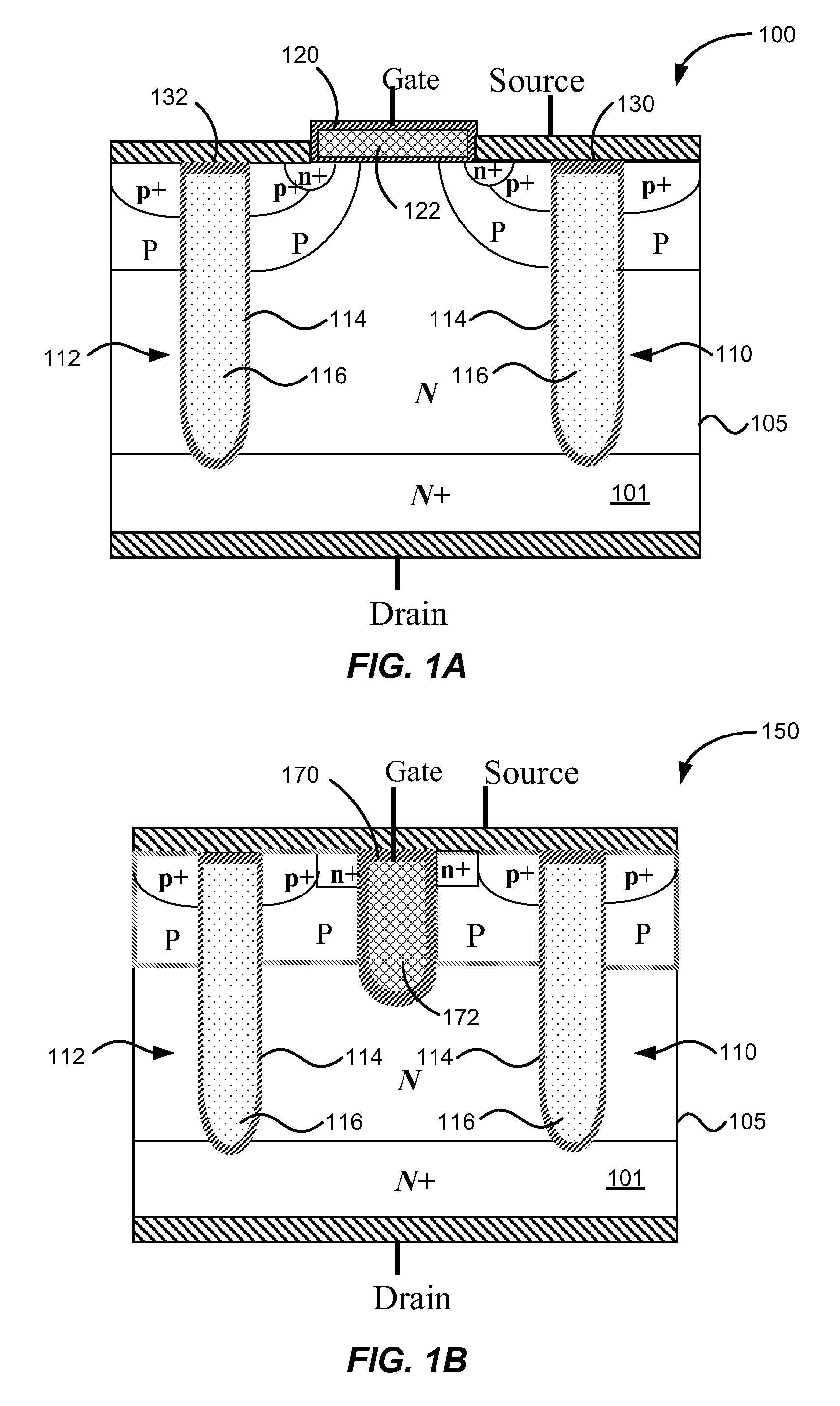
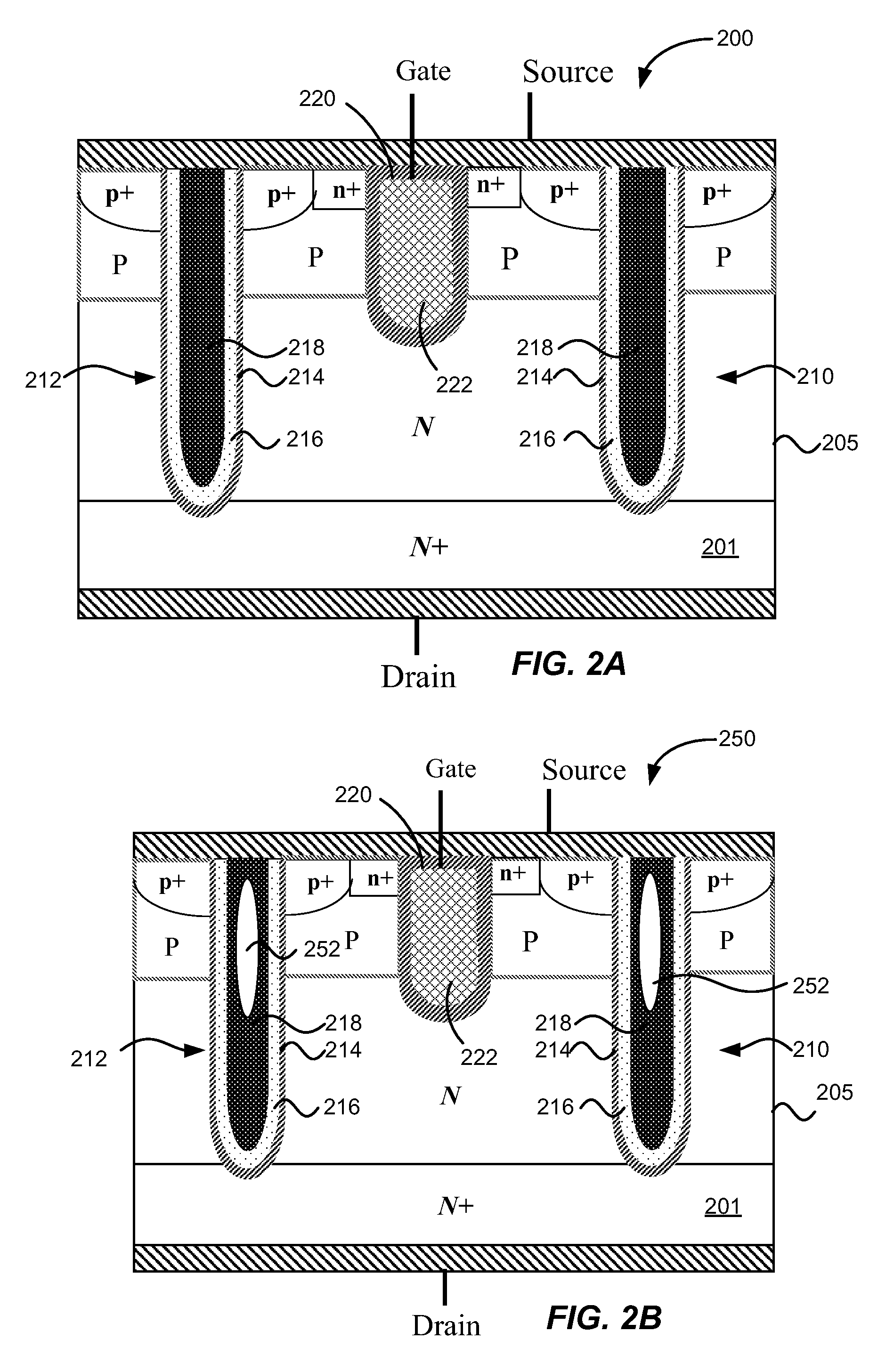
[0118]According to embodiments of the present invention, a power MOSFET structure is provided that is characterized by improved conduction and switching performance. In a particular embodiment, a high voltage MOSFET structure is provided in which dielectric layers containing charge are used to balance the charge in the drift region. By alternating dielectric and silicon layers that are charge balanced, the structure's performance exceeds the one dimensional silicon breakdown voltage limit for a given doping concentration. Both vertical and lateral MOSFET structures are provided by embodiments of the present invention. Furthermore, in a specific embodiment, a lateral structure is used in which dielectric layers with charge are combined with double or multiple Reduced SURface Field (Resurf) techniques for additional improvement in breakdown voltage and / or on-resistance. Methods of fabricating these structures are described and further details, embodiments and examples of the invention...


PUM


Abstract

A semiconductor device includes a semiconductor layer of a first conductivity type and a semiconductor layer of a second conductivity type formed thereon. The semiconductor device also includes a body layer extending a first predetermined distance into the semiconductor layer of the second conductivity type and a pair of trenches extending a second predetermined distance into the semiconductor layer of the second conductivity type. Each of the pair of trenches consists essentially of a dielectric material disposed therein and a concentration of doping impurities present in the semiconductor layer of the second conductivity type and a distance between the pair of trenches define an electrical characteristic of the semiconductor device. The semiconductor device further includes a control gate coupled to the semiconductor layer of the second conductivity type and a source region coupled to the semiconductor layer of the second conductivity type.

Description

CROSS-REFERENCES TO RELATED APPLICATIONS[0001]The present application claims benefit under 35 U.S.C. §119(e) of U.S. Provisional Patent Application No. 60 / 879,434, filed Jan. 9, 2007, entitled “Power MOS Transistor,” the disclosure of which is incorporated herein by reference in its entirety.[0002]The present application is related to co-pending and commonly assigned U.S. patent application Ser. No. 11 / 971,096, filed on Jan. 8, 2008, entitled “Semiconductor device,” the disclosure of which is hereby incorporated by reference for all purposes.[0003]The following four regular U.S. patent applications (including this one) are being filed concurrently, and the entire disclosure of the other applications are incorporated by reference into this application for all purposes:[0004]application Ser. No. ______, filed Jan. 8, 2008, entitled “Semiconductor device” (Attorney Docket No. 027049-000210US);[0005]application Ser. No. ______, filed Jan. 8, 2008, entitled “Semiconductor device” (Attorn...

Claims


Application Information

Patent Timeline
IPC IPC(8): H01L29/78
CPCH01L21/26586H01L29/66666H01L29/0619H01L29/0634H01L29/0653H01L29/0661H01L29/0692H01L29/0696H01L29/0847H01L29/0878H01L29/1095H01L29/408H01L29/4236H01L29/42368H01L29/66734H01L29/7802H01L29/7809H01L29/7811H01L29/7813H01L29/7827H01L29/7835H01L21/2003H01L21/28008H01L21/2658H01L29/66537H01L21/823885H01L21/02164H01L21/0217H01L21/02321H01L21/265H01L21/30604H01L21/324H01L21/76224H01L29/0649
Inventor DARWISH, MOHAMED N.
Owner MAXPOWER SEMICON INC
Why Eureka
Try Eureka