

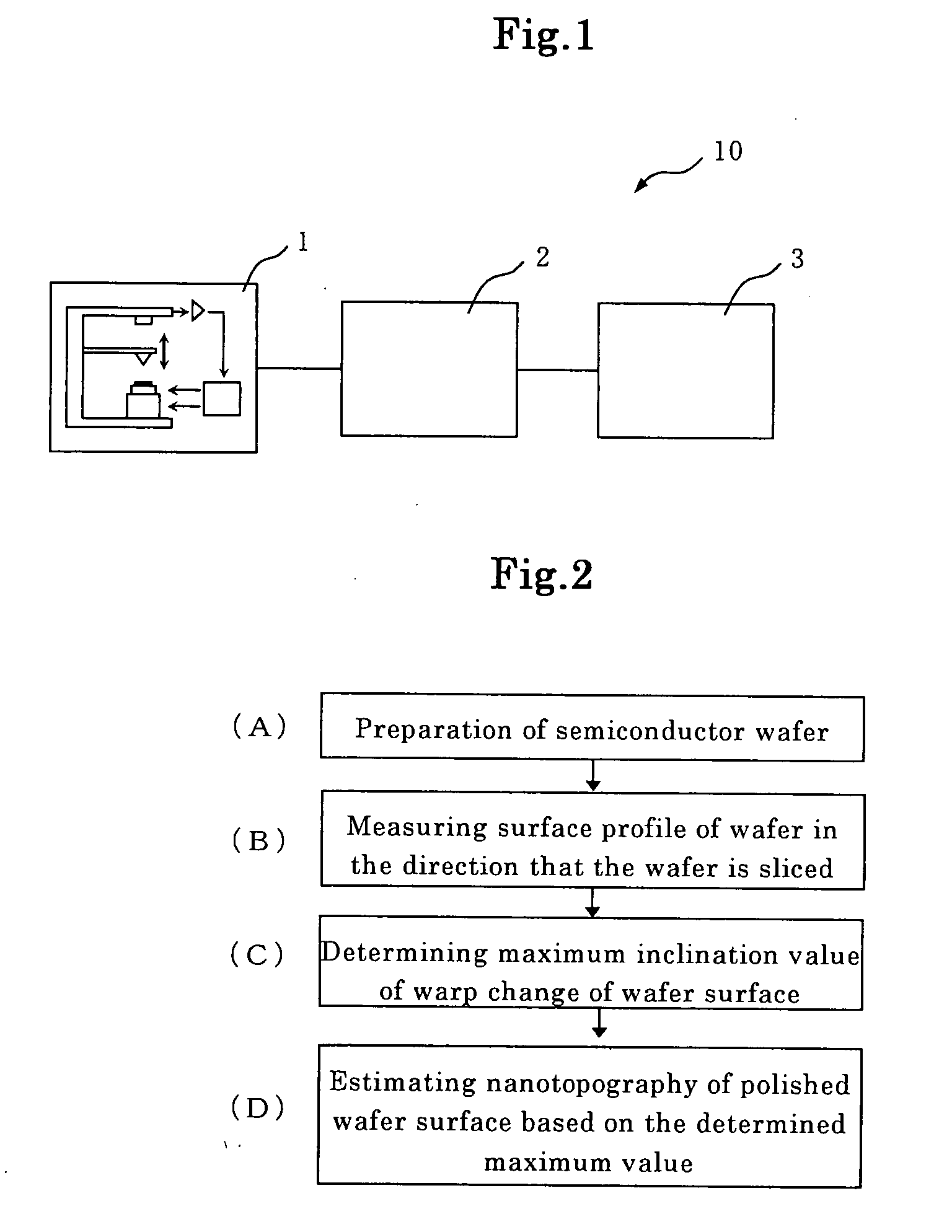
Method for Evaluating Semiconductor Wafer, Apparatus for Evaluating Semiconductor Wafer, and Method for Manufacturing Semiconductor Wafer
- Summary
- Abstract
- Description
- Claims
- Application Information
AI Technical Summary
Benefits of technology
Problems solved by technology
Method used
Image

Examples
experiment 1
(Experiment 1)
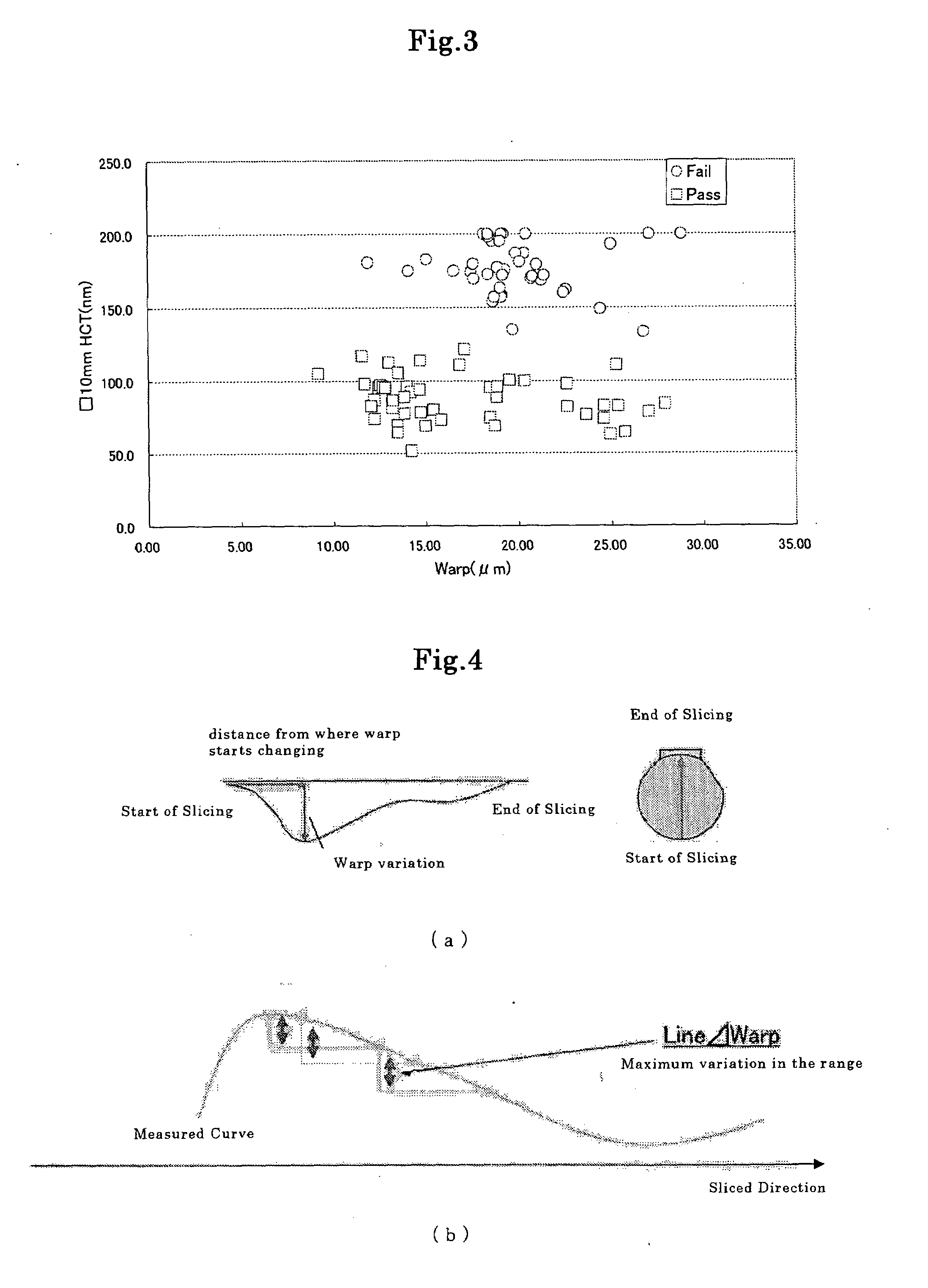
[0058]First, in order to confirm problems of conventional techniques, the present inventors measured the Warp of a silicon wafer surface in the state of as-cut, and determined the correlation between the Warp and nanotopography values of the wafer surface measured after being polished.
[0059]As an indicator for representing nanotopography, HCT was used. HCT is an abbreviation of Height Change Threshold. HCT represents a threshold that is a ratio (% Area) of areas (failure areas) where Height Change among wafer surface heights in square measurement areas in pixel size exceeds a predetermined value to the measurement areas. HCTs were determined by CR83 SQM from ADE Corporation where the pixel size was 10 mm per side and the % Area was 0.5%.
[0060]FIG. 3 shows the results. In FIG. 3, wafers with HCTs equal to or less than 125 nm are judged pass. As shown in FIG. 3, there is no correlation between the Warp in the state of as-cut and nanotopography of the polished wafer. Cons...
experiment 2
(Experiment 2)
[0062]As mentioned above, maximum inclination values of warp change of a wafer surface in the state of as-cut after being sliced and nanotopography of the wafer surface after being polished were determined. The correlation between the maximum inclination values and the nanotopography were determined. As for the maximum inclination value of warp change, various definitions are conceivable. However, in the present invention, definitions of degree of Warp change and Line Δ Warp are newly introduced.
[0063]The Warp change is, as shown in FIG. 4(a), defined as a value obtained by dividing a warp variation by a distance between where the warp starts changing and where the warp finishes changing during the start to the end of slicing of a wafer. The Line Δ Warp is, as shown in FIG. 4(b), a maximum value among variations of heights of the surface obtained in a measurement range being moved, the measurement range being set to have a predetermined width in a sectional profile (a ...
example
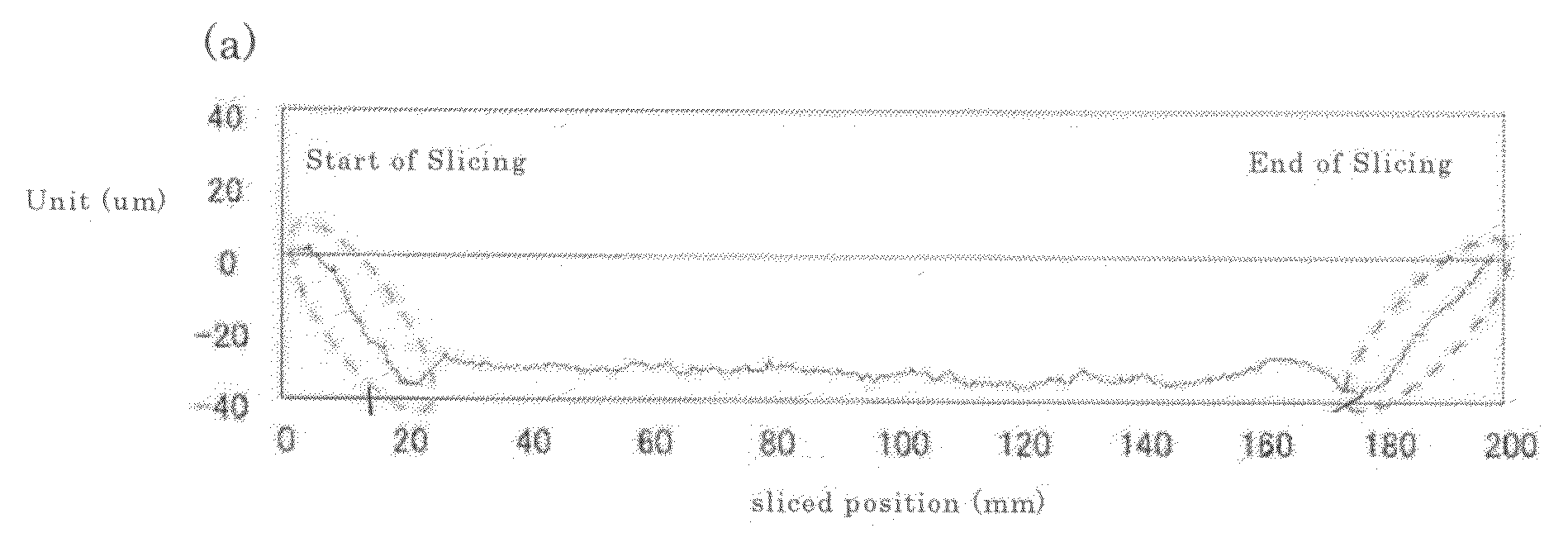
[0100]A silicon wafer was prepared by slicing a silicon single crystal ingot with a diameter of 200 mm grown by CZ method with a wire saw. A surface profile of the wafer in the state of as-cut was measured in the direction that the wafer is sliced with a contact-probe-type profile measuring system. The measurement results are shown in FIG. 8(a). Line Δ Warp was 8.84 μm where the width of a measurement range was 10 mm and the measurement range was moved by a distance of 0.5 mm.
[0101]The Line Δ Warp was larger than 6 μm, which was set as a reference value. Therefore, the wafer was evaluated to be defective in terms of nanotopography after being polished. The wafer was not passed to subsequent steps. In response to the evaluation results of the Line Δ Warp, slicing conditions were adjusted and optimized by adjusting the tension of the wire saw.
[0102]Under the slicing conditions thus optimized, the silicon single crystal ingot was sliced again to prepare a silicon wafer. A surface profi...
PUM
 Abstract
Description
Claims
Application Information