Semiconductor Device and Electronic Device Having the Same

a technology of semiconductor devices and electronic devices, applied in the direction of solid-state devices, basic electric elements, instruments, etc., can solve the problems of easy breakage of parts of antennas and easy attenuation of signals, and achieve the effects of improving mechanical strength of wireless chips, high mechanical strength, and difficult to be blocked

Inactive Publication Date: 2008-07-17
SEMICON ENERGY LAB CO LTD
View PDF29 Cites 68 Cited by
  • Summary
  • Abstract
  • Description
  • Claims
  • Application Information

AI Technical Summary

Benefits of technology

[0027]The layer having the thin film transistor can be formed so as to have almost the same area as the antenna. The antenna serves as a protector for the layer having the thin film transistor. Therefore, the mechanical strength of the wireless chip is improved.
[0028]Since a patch antenna has high mechanical strength, the patch antenna can be reused. Therefore, a wireless chip can be provided on a recyclable container such as a returnable container.
[0029]Further, since a wireless chip of the present invention is formed using an electrically-isolated thin film integrated circuit, an electric wave is more difficult to be blocked than in a wireless chip having an integrated circuit formed using a semiconductor substrate, thereby suppressing the attenuation of a signal due to the block of an electric wave. Thus, it is possible to send and receive data with high efficiency.
[0030]As to a wireless chip including an integrated circuit which is formed using a thin film transistor and a passive element formed with a thick film pattern, each circuit can be formed using an element having a suitable function. By mounting a wireless chip of the present invention to a wiring substrate, the number of mount parts can be decreased; thus, the area of a wiring substrate can be reduced and the electronic device having the wiring substrate can be miniaturized accordingly.

Problems solved by technology

The antenna attached to a flexible material such as paper or plastic has a problem in that the antenna is sensitive to bending or folding, so that a part of the antenna is easily broken.
Moreover, in the case of a wireless chip formed using a semiconductor substrate, the semiconductor substrate serves as a conductor and blocks for an electric wave; therefore, there is a problem that a signal is easily attenuated depending on the direction of a signal which is sent.

Method used


Image

  • Semiconductor Device and Electronic Device Having the Same
  • Semiconductor Device and Electronic Device Having the Same
  • Semiconductor Device and Electronic Device Having the Same

Examples


embodiment mode 1

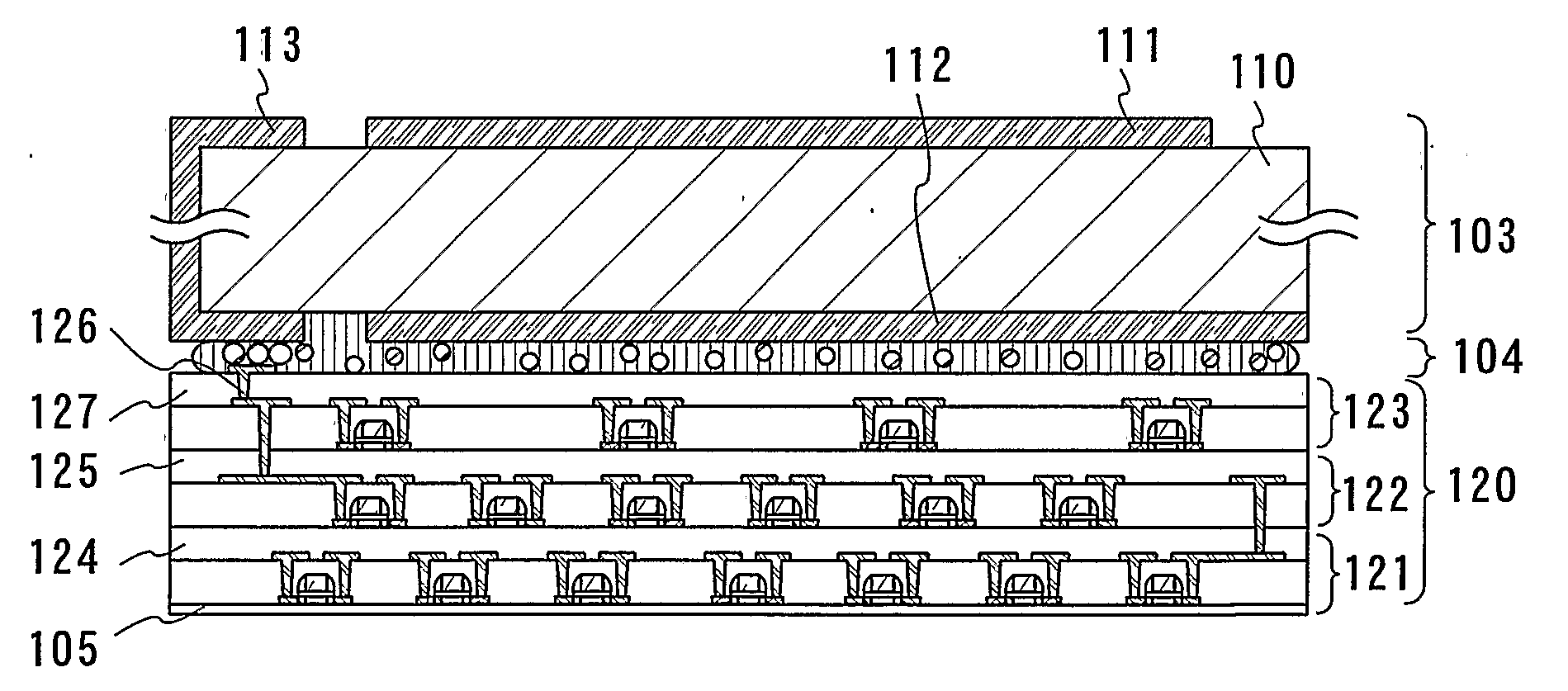
[0056]An embodiment mode of a wireless chip of the present invention is shown in FIGS. 1A and 1B. FIGS. 1A and 1B are cross-sectional views each showing a wireless chip.

[0057]In a wireless chip of this embodiment mode, a layer 102 having a thin film transistor is fixed to an antenna 103 with an anisotropic conductive adhesive 104. Moreover, a connection terminal 107 of the layer 102 having a thin film transistor and a power feeding layer 113 of the antenna are electrically connected by conductive particles 109 dispersed in the anisotropic conductive adhesive 104. Further, although not shown, a ground wiring of the layer having a thin film transistor is electrically connected to a conductive layer serving as a ground contact body of the antenna by the conductive particles 109 dispersed in the anisotropic conductive adhesive 104.

[0058]The layer 102 having a thin film transistor includes a thin film transistor 106 formed over the insulating layer 105, an interlayer insulating layer 108...

embodiment mode 2

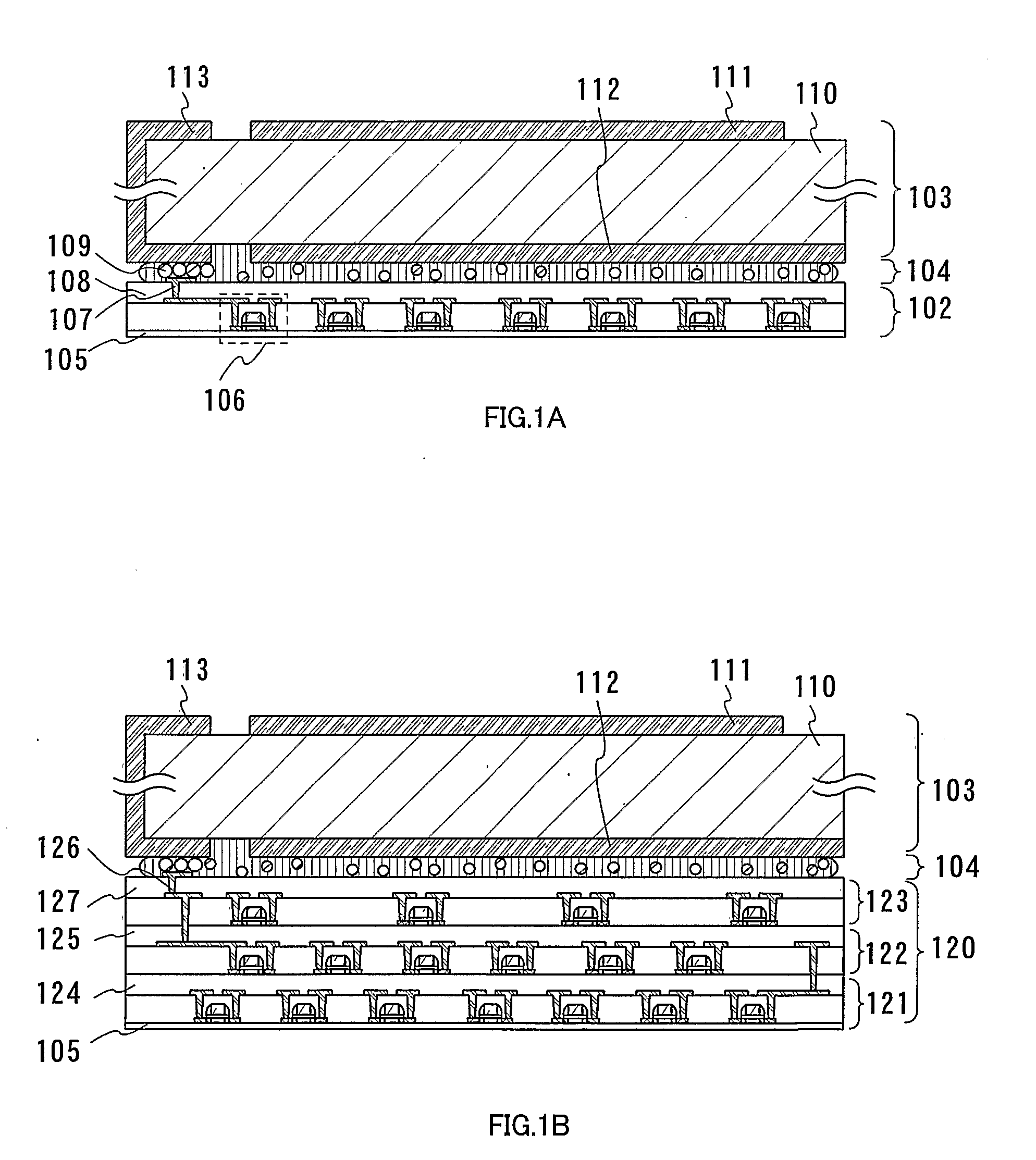
[0135]An embodiment mode of a wireless chip of the present invention will be shown in FIG. 2. FIG. 2 is a cross-sectional view of a wireless chip. In this embodiment mode, a structure of a wireless chip which has a patch antenna and a plurality of layers having thin film transistors wherein the layers are fixed to each other with an anisotropic conductive adhesive will be described.

[0136]In a wireless chip of this embodiment mode, a first layer 102 having a thin film transistor and a second layer 131 having a thin film transistor are fixed to each other with an anisotropic conductive adhesive 133.

[0137]A first connection terminal formed on the surface of the first layer 102 having a thin film transistor is electrically connected to a second connection terminal formed on the surface of the second layer 131 having a thin film transistor through conductive particles dispersed in the anisotropic conductive adhesive 133.

[0138]Similarly to the first layer 102 having a thin film transistor...

embodiment mode 3

[0147]An embodiment mode of a wireless chip of the present invention will be described with reference to FIG. 4. FIG. 4 is a cross-sectional view of a wireless chip. This embodiment mode will describe a structure of a wireless chip in which a layer having a thin film transistor, a passive element, and a patch antenna are fixed to each other with an anisotropic conductive adhesive, a conductive layer, or the like.

[0148]As shown in Embodiment Mode 1, the layer 102 having a thin film transistor is formed. The layer 102 having a thin film transistor and the passive element 150 are fixed to each other with the anisotropic conductive adhesive 104. Here, the passive element 150 is shown as a first passive element 151 and a second passive element 152. Further, the connection terminal 107 exposed at the surface of the layer 102 having a thin film transistor is electrically connected to a first connection terminal 160 of the passive element 150 by conductive particles in the anisotropic condu...


PUM


Abstract

It is an object of the present invention to provide a wireless chip of which mechanical strength can be increased. Moreover, it is an object of the present invention to provide a wireless chip which can prevent an electric wave from being blocked. The invention is a wireless chip in which a layer having a thin film transistor is fixed to an antenna by an anisotropic conductive adhesive or a conductive layer, and the thin film transistor is connected to the antenna. The antenna has a dielectric layer, a first conductive layer, and a second conductive layer. The dielectric layer is sandwiched between the first conductive layer and the second conductive layer. The first conductive layer serves as a radiating electrode and the second conductive layer serves as a ground contact body.

Description

TECHNICAL FIELD[0001]The present invention relates to a wireless chip by which data can be sent and received through wireless communication and an electronic device having the wireless chip.BACKGROUND ART[0002]In recent years, of a wireless chip including a plurality of circuits and an antenna has been developed. Such a wireless chip is referred to as an ID tag, an IC tag, an IC chip, an RF (Radio Frequency) tag, a wireless tag, an electronic tag, an RFID (Radio Frequency IDentification) tag, or the like and has already been introduced into some markets.[0003]Many of these wireless chips which are currently in practical use have circuits using semiconductor substrates of silicon or the like (such circuits are also referred to as IC (Integrated Circuit) chips) and antennas. The antenna is formed by a printing method, a method in which a conductive thin film is etched, a plating method, or the like (for example, Patent Document 1: Japanese Patent Application Laid-Open No. H9-1970).[00...

Claims


Application Information

Patent Timeline
Patent Type & Authority Applications(United States)
IPC IPC(8): G06K19/077
CPCH01L21/84H01L27/105H01L27/1214H01L27/1266H01Q23/00H01L27/1052H01L2224/83005H01L2224/2912H01L2224/2939H01L2224/29439H01L2224/29447H01L21/6836H01L24/83H01L24/97H01L2221/68327H01L2221/6835H01L2221/68377H01L2221/68381H01L2224/06181H01L2224/29109H01L2224/29111H01L2224/29139H01L2224/29147H01L2224/29364H01L2224/32225H01L2224/83007H01L2224/83851H01L2224/97H01L2224/29155H01L2224/29118H01L2224/29113H01L2224/29444H01L2224/29464H01L2224/03002H01L2224/32265H01L2924/142H01L23/64H01L23/66H01L24/29H01L25/0657H01L25/16H01L2223/6677H01L2224/2929H01L2224/29339H01L2224/29344H01L2224/29347H01L2224/32145H01L2224/33181H01L2224/94H01L2924/19041H01L2924/19042H01L2924/19043H01L2924/19104H01L2225/06513H01L2225/06565H01L2224/03009H01L24/32H01L2224/32501H01L2924/07811H01L2924/00H01L2224/03H01L2924/0665H01L2924/00014H01L2924/014H01L2224/83H01L2924/15788H01L2924/12042H01L2924/12044H01L2924/14H10B99/00H01L27/0688H01L27/12
Inventor SUZUKI, YUKIEARAI, YASUYUKIYAMAZAKI, SHUNPEI
Owner SEMICON ENERGY LAB CO LTD
Why Eureka
Try Eureka