Semiconductor device having conductive bumps and fabrication method thereof
- Summary
- Abstract
- Description
- Claims
- Application Information
AI Technical Summary
Benefits of technology
Problems solved by technology
Method used
Image

Examples
first embodiment
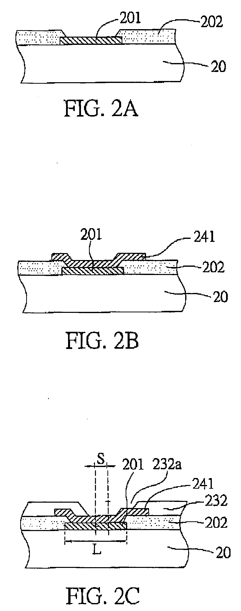
[0027]Please refer to FIGS. 2A to 2E, which are sectional views showing a semiconductor device having conductive bumps and a fabrication method thereof according to a first embodiment of the present invention.
[0028]As shown in FIG. 2A, a semiconductor substrate 20 is provided and has a plurality of solder pads 201 and a passivation layer 202 preformed on the semiconductor substrate 20 (for simplifying the descriptions, an area with single solder pad 201 is illustrated), where the semiconductor substrate 20 is, for example, a semiconductor chip or a wafer that has a plurality of chips, a surface of the semiconductor substrate 20 is covered with the passivation layer 202, and the passivation layer 202 has an aperture for exposing the solder pad 201 therefrom. The material of the passivation layer 202 is, for example, polyamide (PI) or silicon nitride, for protecting the semiconductor substrate 20.
[0029]As shown in FIG. 2B, a first metal layer 241 is formed directly on the passivation ...
second embodiment
[0035]Please refer to FIG. 3, which is a sectional view showing a semiconductor device having conductive bumps according to a second embodiment of the present invention. The semiconductor device having conductive bumps of the present embodiment is similar to that in the first embodiment, the major difference therebetween is that the semiconductor device having conductive bumps of the present embodiment further comprising another covering layer disposed on the passivation layer, which is useful when the material of the passivation layer of the semiconductor substrate is, for example, a nitride (such as silicon nitride).
[0036]As shown in FIG. 3, the semiconductor device having conductive bumps of the present embodiment comprises: a semiconductor substrate 30, a plurality of solder pads 301 (only one is illustrated for simplifying the description) and a passivation layer 302 formed on a surface of the semiconductor substrate 30; a covering layer 331 disposed on the passivation layer 30...
third embodiment
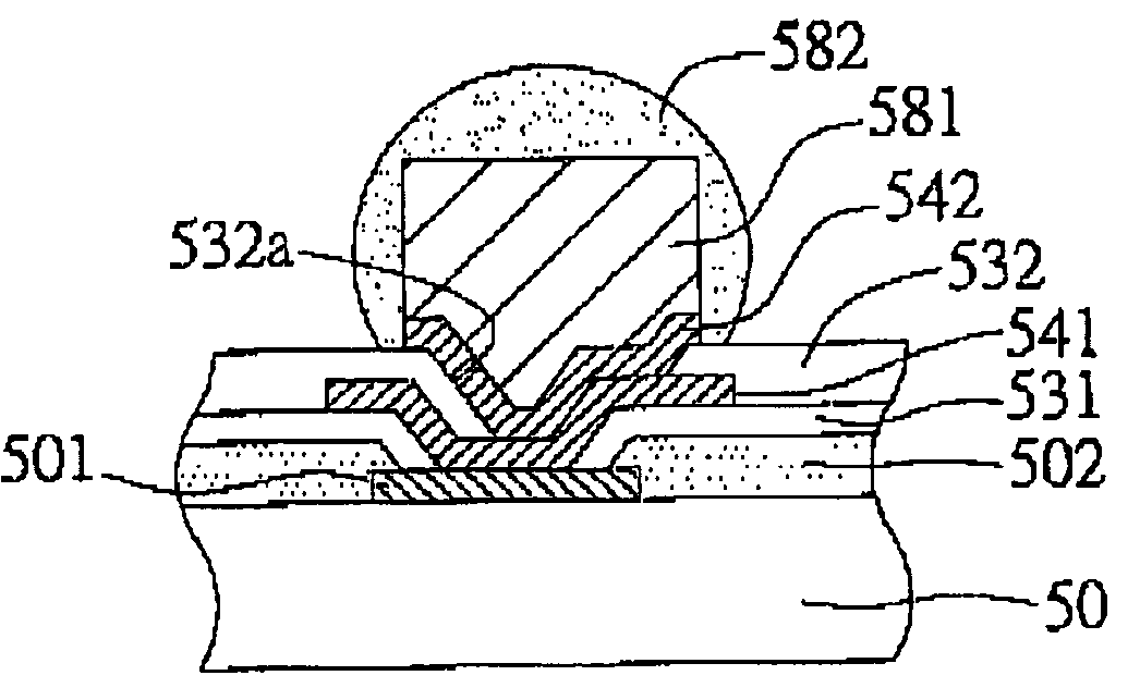
[0038]Pleaser refer to FIG. 4, which is a sectional view showing a semiconductor device having conductive bumps according to a third embodiment of the present invention. The semiconductor device having conductive bumps of the present embodiment is similar to that in the first embodiment, the major differences therebetween are that the semiconductor device having conductive bumps of the present embodiment further comprising another metal layer. A shown in FIG. 4, a first metal layer 441′ is directly disposed on top of the solder pad 401 and a passivation layer 402, which are both formed on a surface of a semiconductor substrate 40, so as to electrically connect the first metal layer 441 to a portion of the solder pad 401 which is exposed from the passivation layer 402. Next, a covering layer 432 is disposed on the first metal layer 441 and the passivation layer 402, wherein the coveting layer 432 having an aperture 432a formed therein for exposing a portion of the first metal layer 4...
PUM
 Abstract
Description
Claims
Application Information