
Thin film bulk acoustic wave resonator structure and filter, and radio-frequency module using them

a resonator and bulk technology, applied in piezoelectric/electrostrictive/magnetostrictive devices, piezoelectric/electrostriction/magnetostriction machines, electrical apparatus, etc., can solve the problems of difficult or impossible to design a band-pass filter, difficult or impossible to achieve compatibility with semiconductor processes, and increase in cost. , to achieve the effect of reducing the element area, wide pass, and low insertion loss

Inactive Publication Date: 2008-07-17
HITACHI MEDIA ELECTORONICS CO LTD
View PDF6 Cites 49 Cited by
  • Summary
  • Abstract
  • Description
  • Claims
  • Application Information

AI Technical Summary

Benefits of technology

[0006]Along with the progress of technology for mobile communication systems including mobile telephones, smaller and less costly radio-frequency filters subject to a low insertion loss and having a wide pass band are called for.
[0009]Referring now to U.S. Pat. No. 5,587,620, the statement that “Electrode 26 common to both FBARs” in U.S. Pat. No. 7,019,605 B2 can be construed as meaning that the central electrode 26 is grounded. U.S. Pat. No. 7,019,605 B2, in view of the circumstance that the technique disclosed in U.S. Pat. No. 5,587,620 cited above “The single Lorentzian resonance makes it difficult or impossible to design a band-pass filter with such desirable characteristics such as broad pass hand”, attempts to provide the band-pass filter such desirable properties as a low insertion loss and flat frequency response in its pass band, a pass bandwidth in the range from about 3% to about 5% of the center frequency and good out-of-band rejection by the reduced acoustic coupling.
[0011]The present invention is intended to address these problems with conventionally available techniques. The main problem to be addressed by the invention is to realize a reduction in element area without relying on highly difficult manufacturing techniques to produce a BAW resonator structure and radio-frequency filter subject to a low insertion loss and having a wide pass band.
[0013]The BAW resonator structure and the radio-frequency filter according to the invention allow a substantial reduction in element area by arraying a plurality of BAW resonators in the height direction. Also according to the invention, it is made possible to configure a filter by electrically connecting a plurality of BAW resonators, and a radio-frequency filter subject to a low insertion loss and having a wide pass band, such as a ladder circuit, can be fabricated.

Problems solved by technology

However, it requires a manufacturing process using a sacrificial layer to form a hollow structure.
This entails the problem of requiring difficult manufacturing techniques and accordingly an increase in cost.
There is another disadvantage that, since no process to form a hollow structure is used for semiconductor device manufacturing in general, it is difficult to achieve compatibility with semiconductor processes.
U.S. Pat. No. 7,019,605 B2, in view of the circumstance that the technique disclosed in U.S. Pat. No. 5,587,620 cited above “The single Lorentzian resonance makes it difficult or impossible to design a band-pass filter with such desirable characteristics such as broad pass hand”, attempts to provide the band-pass filter such desirable properties as a low insertion loss and flat frequency response in its pass band, a pass bandwidth in the range from about 3% to about 5% of the center frequency and good out-of-band rejection by the reduced acoustic coupling.

Method used


Image

  • Thin film bulk acoustic wave resonator structure and filter, and radio-frequency module using them
  • Thin film bulk acoustic wave resonator structure and filter, and radio-frequency module using them
  • Thin film bulk acoustic wave resonator structure and filter, and radio-frequency module using them

Examples


embodiment 1

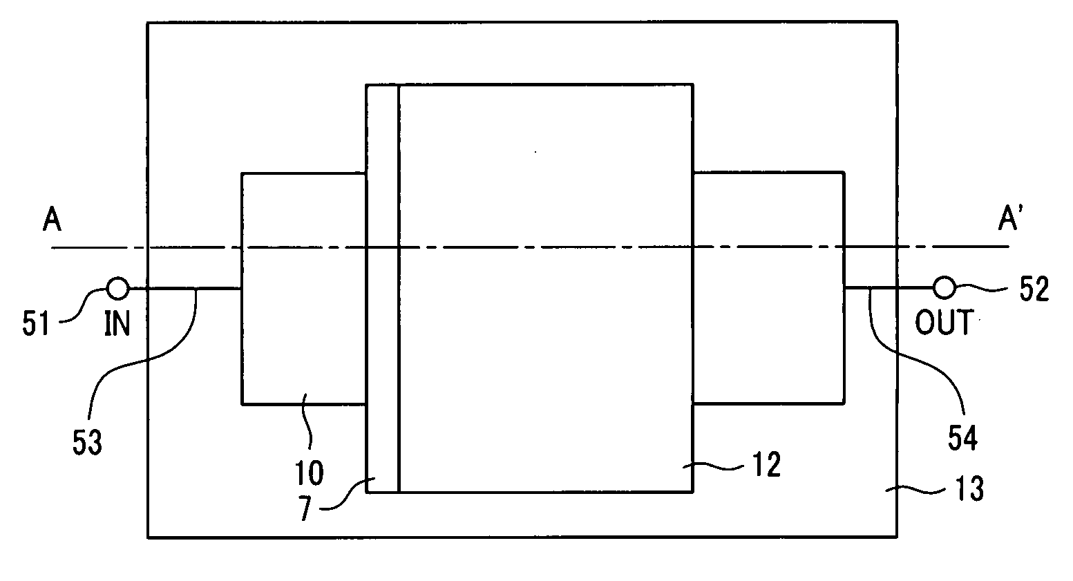
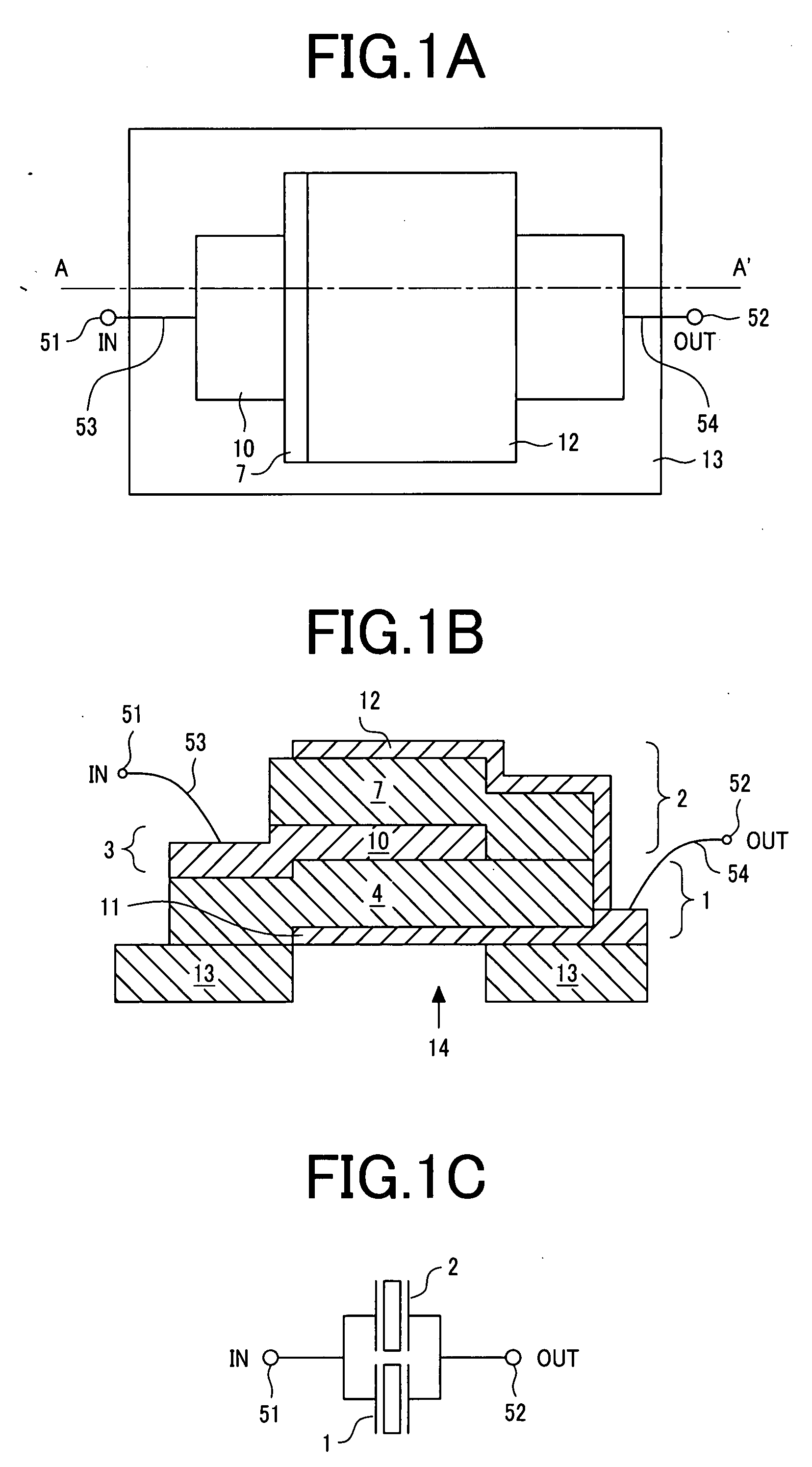
[0055]First, a first preferred embodiment of the invention will be described with reference to FIG. 1A to FIG. 1D, FIG. 2, and FIG. 3. FIG. 1A to FIG. 1C show a BAW resonator structure, which is one embodiment of the invention, wherein FIG. 1A shows a plan view of the resonator structure; FIG. 1B, an A-A′ section view of FIG. 1A; and FIG. 1C, an equivalent circuit to the structure shown in FIG. 1A and FIG. 1B.

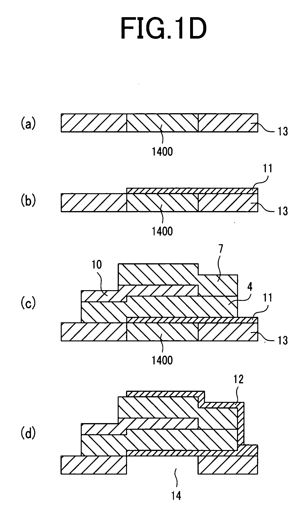
[0056]The BAW resonator structure of this embodiment is provided with a first BAW resonator 1, an electroconductive acoustic reflection layer 3, a second BAW resonator 2 and a cavity 14 disposed in a substrate 13. The first BAW resonator 1 includes a first piezoelectric layer 4, and a first metal layer 11 and a second metal layer 10 placed underneath the lower face and over the upper face of this first piezoelectric layer 4. The second BAW resonator 2 includes a second piezoelectric layer 7, and a second metal layer 10 and a third metal layer 12 placed underneath the lower face...

embodiment 2

[0090]Next, a radio-frequency filter which has a BAW resonator which is a second preferred embodiment of the invention will be described with reference to FIG. 6A to FIG. 6C, wherein FIG. 6A shows a plan view of the filter; FIG. 6B an A-A′ section of FIG. 6A; and FIG. 6C, an equivalent circuit to the filter having the configuration of this embodiment.

[0091]The BAW resonator of this embodiment is provided with the first piezoelectric layer 4, the second piezoelectric layer 7, the first electrode 10 including the electroconductive acoustic reflection layer and connected to the input terminal 51, the second electrode 11, the third electrode 12, the substrate 13 and the cavity 14. It is desirable for the cavity 14 to extend over the most or whole part of the bottom face of the area in which the first electrode 10 and the second electrode 11 overlap each other. The differences from Embodiment 1 include the difference in film thickness between the first piezoelectric layer 4 and the secon...

embodiment 3

[0100]FIG. 8 shows a section view of a BAW resonator structure, which is another preferred embodiment applicable to the resonator structure and filter described with reference to the first and second embodiments of the invention and other BAW resonator structures embodying the invention in other ways to be described afterwards. This BAW resonator structure is provided with the substrate 13, the first BAW resonator 1, the electroconductive acoustic reflection layer 3 and the second BAW resonator 2, wherein the first BAW resonator 1 includes the first piezoelectric layer 4 and a first metal layer 19 placed underneath the lower face of the first piezoelectric layer 4, and the second BAW resonator 2 includes the second piezoelectric layer 7 and a fourth metal layer 20 placed over the upper face of the second piezoelectric layer 7. The electroconductive acoustic reflection layer 3 constitutes the first electrode, the first metal layer 19 constitutes the second electrode, and the fourth m...


PUM


Abstract

A thin film bulk acoustic wave (BAW) resonator structure and filter which can be fabricated by inexpensive manufacturing techniques and in smaller size than conventional such products are to be provided. The BAW resonator structure and filter have a substrate, a first BAW resonator placed over the substrate, an acoustic reflection layer placed over the first BAW resonator and a second BAW resonator placed over the acoustic reflection layer, and the acoustic reflection layer is electroconductive. Herein, the acoustic reflection layer constitutes a first electrode, and this first electrode electrically connects and acoustically separates the first BAW resonator and the second BAW resonator.

Description

CLAIM OF PRIORITY[0001]The present invention application claims priority from Japanese application JP2007-6102 filed on Jan. 15, 2007, the content of which is hereby incorporated by reference into this application.FIELD OF THE INVENTION[0002]The present invention relates to a thin film bulk acoustic wave resonator (BAW resonator) structure and a bulk acoustic wave filter (BAW filter), and a radio-frequency module using them.BACKGROUND OF THE INVENTION[0003]BAW resonators are applicable to frequency bands of a few hundred MHz to more than 10 GHz, and examples of their application include the use of BAW resonators in the configuration of a radio-frequency filter in a mobile communication system such as mobile telephones (see, for instance, Electronics Letters, Vol. 35, pp. 794-795, 1999).[0004]Known techniques for downsizing BAW resonators and filters include one by which BAW resonators are divided in the perpendicular direction (see U.S. Pat. No. 7,038,559 B2).[0005]Also, U.S. Pat. N...

Claims


Application Information

Patent Timeline
IPC IPC(8): H03H9/54H03H9/17H04B1/3822H04B1/40
CPCH03H3/04H03H9/0095H03H9/583H03H9/605H03H9/585H03H9/588H03H9/589H03H9/584
Inventor MATSUMOTO, HISANORIISOBE, ATSUSHIASAI, KENGO
Owner HITACHI MEDIA ELECTORONICS CO LTD
Learn More