MIM capacitor and metal gate transistor

a metal gate transistor and capacitor technology, applied in the field of metal-insulator-metal (mim) capacitor structure, can solve the problems of pip capacitors with unacceptable performance including unstable capacitance with varying applied voltage, pip capacitors with additional shortcoming, and difficult to manufactur

Active Publication Date: 2008-07-24
TAIWAN SEMICON MFG CO LTD
View PDF11 Cites 45 Cited by
  • Summary
  • Abstract
  • Description
  • Claims
  • Application Information

AI Technical Summary

Benefits of technology

[0008]Thus, an improved MIM capacitor structure and manufacturing process achieving reduced cost and improved performance of both MIM capacitors and CMOS transistors including mixed mode systems is desirable.

Problems solved by technology

Formation of PIP capacitors is, however, problematic in CMOS process technologies used to form a logic circuit on an adjacent region of a chip.
In addition, PIP capacitors have unacceptable performance including unstable capacitance with varying applied voltages, primarily due to carrier depletion effects.
Moreover, PIP capacitors have the additional shortcoming of difficult scale down as well as exhibiting poor performance in high speed applications.
Thus, these and other shortcomings make PIP capacitors undesirable for use in future mixed mode circuitry applications.
Several conventional difficulties conventional processes remain to be overcome.
For example, MIM capacitors are generally formed as BEOL processes, adding to processing steps and cost, as well as presenting process integration challenges with both FEOL and BEOL CMOS processes including damascene interconnect processes.
Electronic mismatching of circuitry components results in degraded signal processing quality and is adversely affected by deviations in critical dimensions between components.

Method used


Image

  • MIM capacitor and metal gate transistor
  • MIM capacitor and metal gate transistor
  • MIM capacitor and metal gate transistor

Examples


Embodiment Construction

[0020]The following description is of the best-contemplated mode of carrying out the invention. This description is made for the purpose of illustrating the general principles of the invention and should not be taken in a limiting sense. The scope of the invention is best determined by reference to the appended claims.

[0021]While the embedded MIM capacitor structure and method for forming the same according to the invention is described with reference to an exemplary mixed mode device including an adjacent CMOS transistor (e.g., MOSFET) device (e.g., on the same chip), It will be appreciated by those skilled in the art that the method of the invention may be used in the formation of other devices including adjacent capacitors (charge storing devices) and transistors such as analog RF circuitry and DRAM devices, where an MIM capacitor structure and transistor gate structure are advantageously formed in parallel.

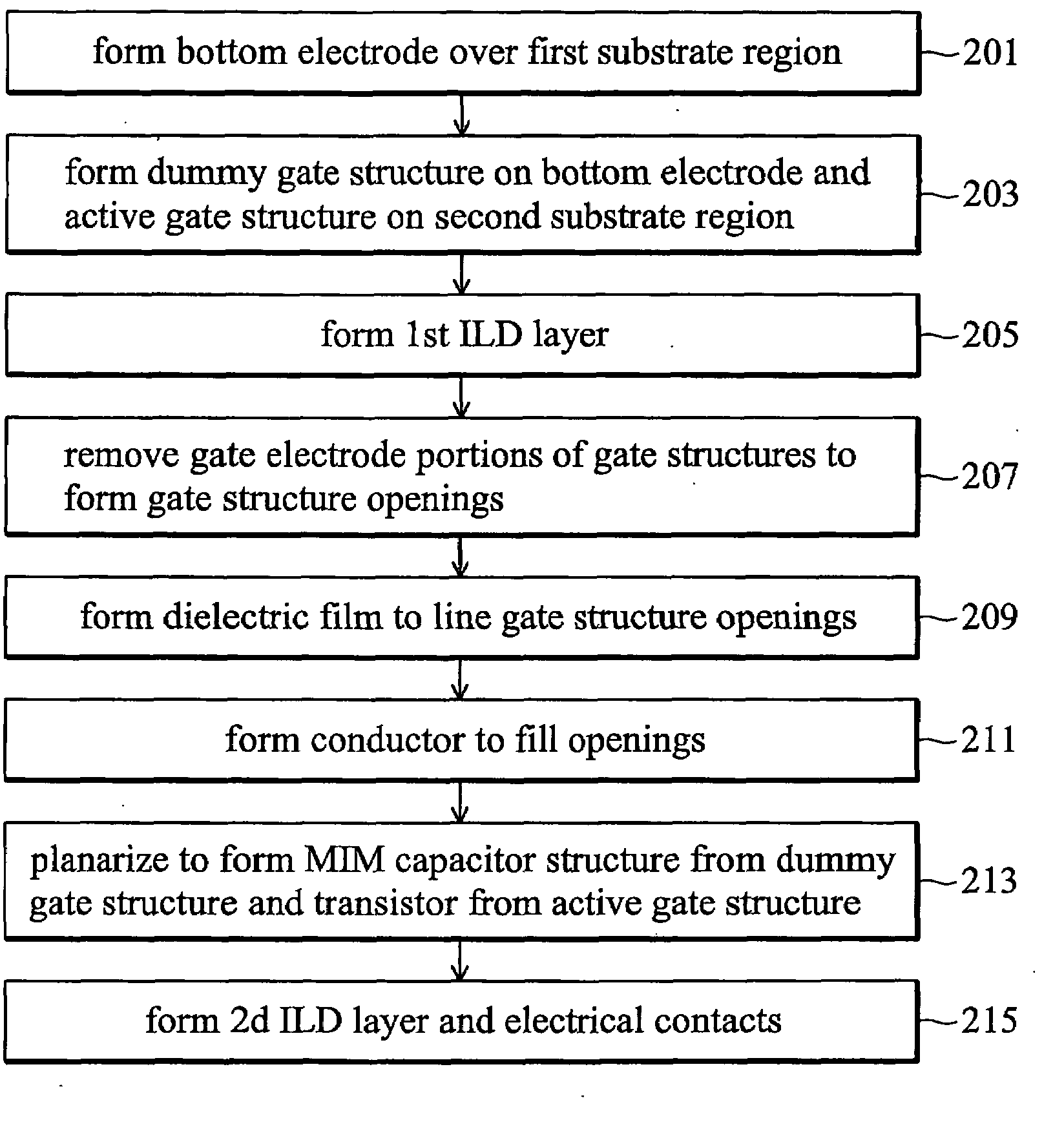
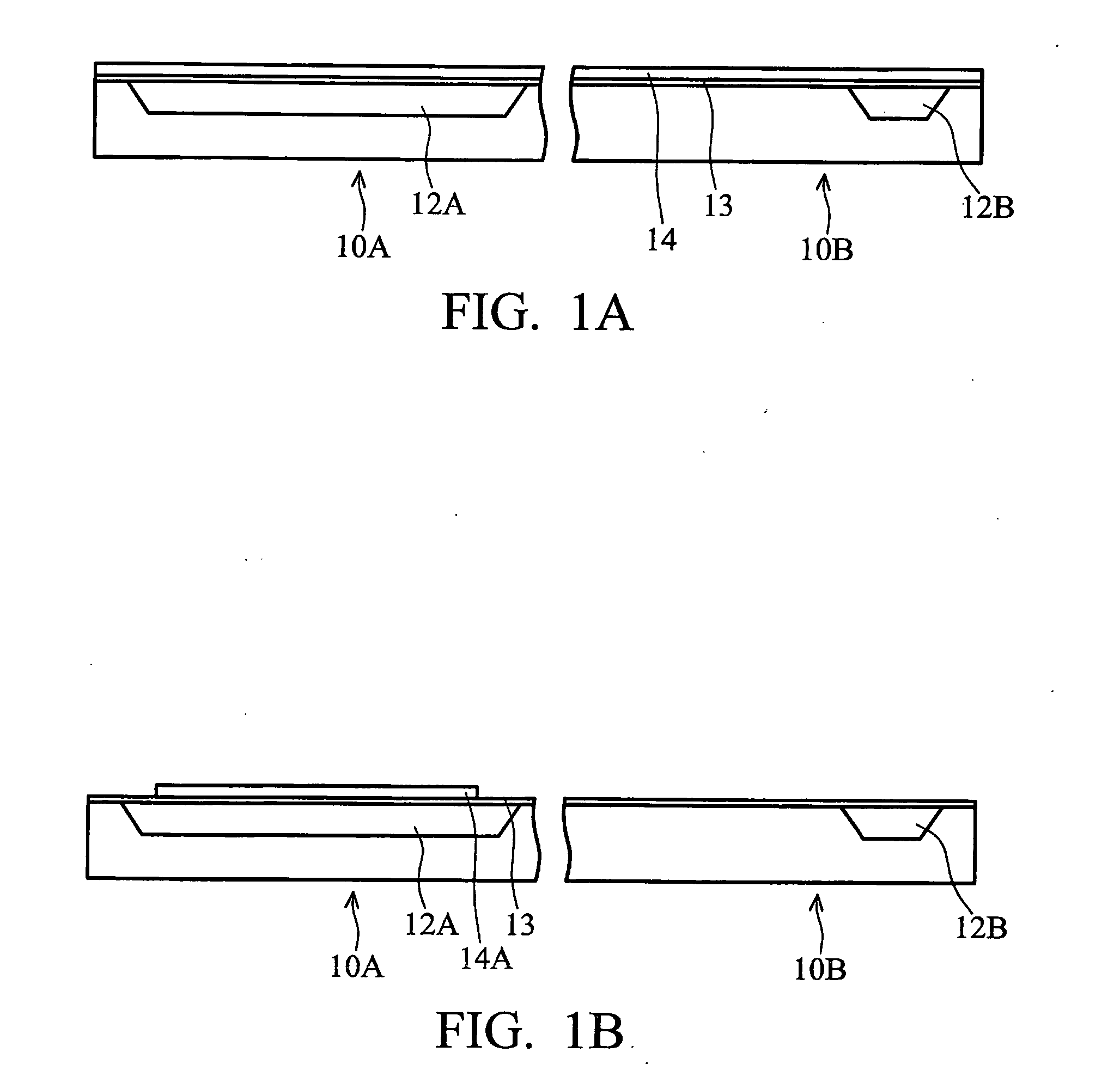
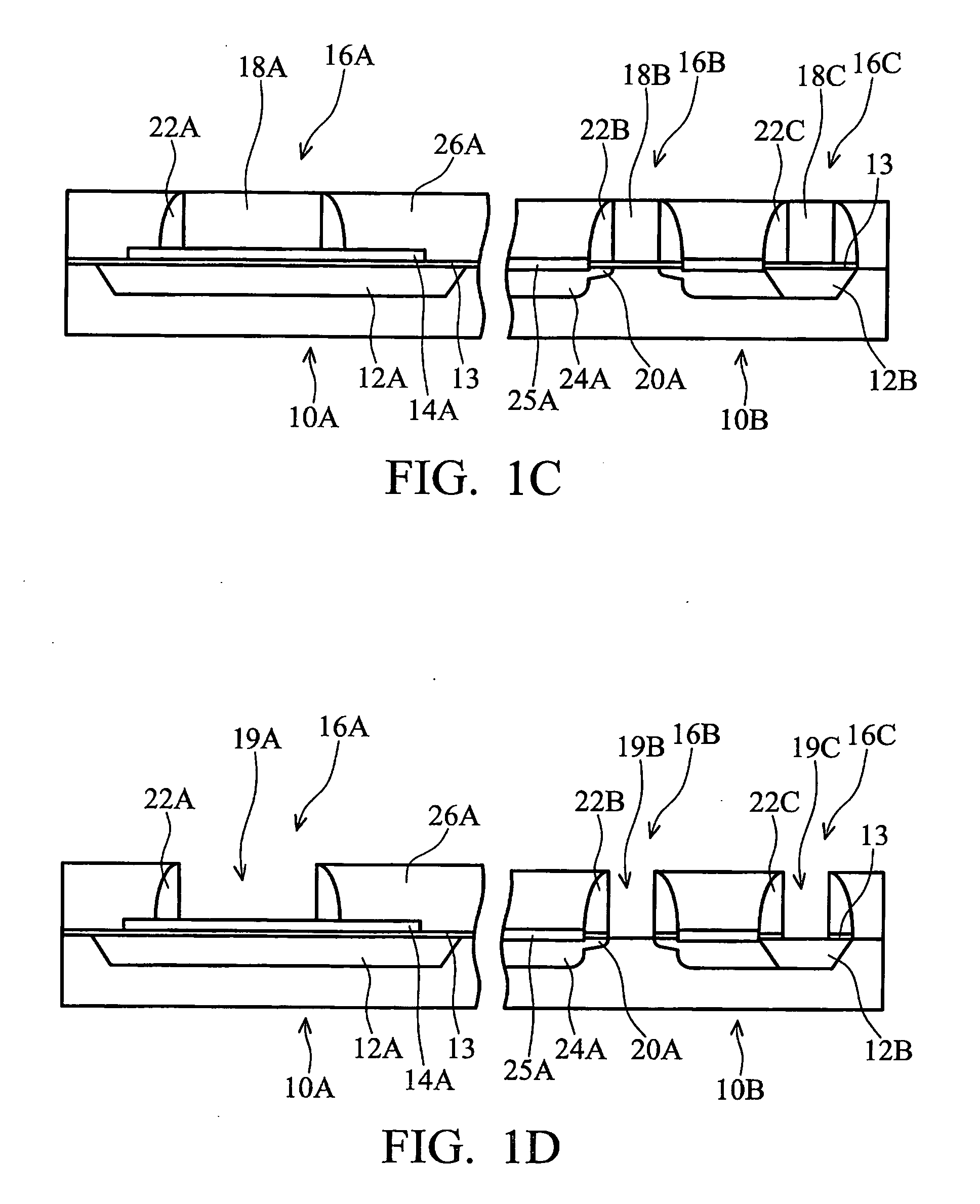
[0022]FIGS. 1A-1G show an exemplary embodiment of the invention at stages...


PUM


Abstract

An embedded MIM capacitor in a logic circuit and method for forming the same are disclosed. The device includes a substrate, a bottom electrode, a dielectric film, and a top electrode. The substrate comprises an insulator region. The bottom electrode comprises a first conductor and overlies the insulator region. The dielectric film overlies the bottom electrode, remaining parts of the bottom plate exposed. The top electrode comprises a second conductor and overlies the dielectric film. The dielectric film lines sidewalls and bottom of the top electrode.

Description

BACKGROUND OF THE INVENTION[0001]1. Field of the Invention[0002]This invention relates to metal-insulator-metal (MIM) capacitor structures and more particularly to a device comprising an MIM capacitor structure and adjacent metal gate electrode CMOS transistor and a method for forming the same in parallel to reduce a processing cost, improve a process flow, and improve both MIM capacitor and CMOS transistor performance in high speed applications.[0003]2. Description of the Related Art[0004]Advances in technology have resulted in an increasing demand for system-on-chip products where both analog and digital signal processing are desirable. Increasingly it is advantageous for both the analog circuitry and digital circuitry to be in close proximity. For example, digital and analog circuitry blocks operating together are referred to as mixed mode systems.[0005]Polysilicon-insulator-polysilicon (PIP) capacitors are well known in the art and have been used in conventional mixed mode syste...

Claims


Application Information

Patent Timeline
Patent Type & Authority Applications(United States)
IPC IPC(8): H01L29/00H01G2/00
CPCH01G4/002H01G4/40H01G13/00H01G17/00H01L29/66545H01L27/0629H01L27/10852H01L28/60H01L21/823828H10B12/033
Inventor TU, KUO-CHI
Owner TAIWAN SEMICON MFG CO LTD
Why Eureka
Try Eureka